Öffnet in neuem Fenster Opens in a new window Öffnet externe Seite Opens an external site Öffnet externe Seite in neuem Fenster Opens an external site in a new window

Institute Silicon Photovoltaics

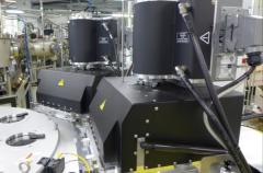
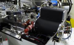
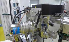
Kobus Deposition cluster

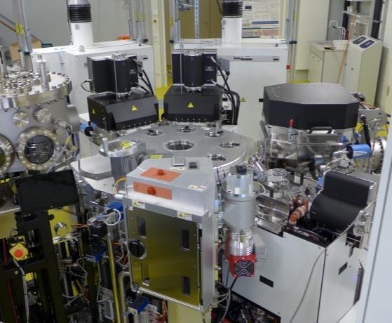
Silicon deposition cluster

Depositions of silicon-related materials in EMIL are carried out in a cluster tool manufactured by the company Kobus, France. In a cluster tool different process chambers are arranged around a central handling chamber, which is equipped with a robot that loads and unloads samples from each individual chamber. Up to ten samples, either wafers up to diameters of 150 mm or square shaped substrates up to 10x10 cm2, can be introduced into the loadlock. This loadlock opens into a flow box ensuring a clean path for  substrates from the neighboring clean room area into the setup.


Tool configuration

The cluster tool comprises four different depositions chambers, two PECVD chambers, one ALD chamber and one PVD chamber. The chambers can be operated in parallel and the whole system is designed to carry out automated process sequences, defined individually for each substrate. This can be used to prepare multiple, identical samples or to carry out experimental series in which deposition parameters like doping or film thickness are varied systematically with minimum user operation required.

An additional chamber of the cluster system is connected to the UHV backbone of the SISSY lab via a sample separation chamber. Wafers or carriers can be lifted into this separation chamber, where a transfer of individual samples to sample carriers of the UHV backbone can be carried out manually under UHV conditions.

PECVD Chambers

The silicon deposition cluster comprises two identical parallel plate PECVD (Plasma Enhanced Chemical Vapor Deposition) chambers. In these chambers precursor gases are introduced in between two electrodes and a plasma is used to activate the gas molecules, causing reactions of the gas molecules with the substrate and chamber walls. A wide range of process gases is available in both deposition chambers, enabling deposition of a variety of silicon based compounds such as amorphous silicon (a-Si:H), microcrystalline silicon (µc-Si:H), silicon nitride, silicon oxide and silicon carbide. PH3, TMB and B2H6 are available as doping sources. Typical thicknesses of films deposited by PECVD are between a few nm and a few 100 nm.


Specially designed ceramic heaters with embedded electrodes allow deposition and chamber etching at temperatures up to 600 °C. The electrode gap distance can be adjusted from 5 to 50 mm. Chamber etching can be carried out via remote plasma activation of the cleaning gases. Plasma cleaning step durations are controlled by optical spectroscopy.


Applications include passivation layers of amorphous silicon, silicon oxide or silicon nitride, emitter and back BSF (back surface field) layers for a-Si:H/c-Si heterojunction solar cells, dielectric coatings, diffusion barriers and optical coatings. Additionally one chamber is prepared for GeH4 introduction, allowing deposition of films based on Germanium or SiGe compounds.

ALD chamber

ALD (Atomic Layer Deposition) is a process, in which films are deposited in a series of consecutive process steps. A precursor gas and an oxidizing gas are alternately introduced into the chamber, with purging steps in between. In each deposition step, the introduced gas reacts with the substrate surface in a self-limiting manner, which means that the interaction between gas and substrate stops once the substrate is covered with precursor or fully reacted with the oxidizing gas. In summary, a sub-monolayer of compound is formed on the substrate and the process is repeated.


As the amount of material deposited per step is very small, a precise control of film thickness is possible by choosing the number of process cycles carried out. In this way film thicknesses can be controlled on a sub-nm scale. On the other hand the nature of the reaction allows highly conformal coating of structured substrates with high aspect ratio.


The ALD chamber of the silicon deposition cluster is equipped with four precursor lines, two for bubblers and two DLI (Direct Liquid Injection) lines. Nitrogen, oxygen, ammonia, hydrogen and ozone are available as reactive gas. Reactive gases can be activated via a remote plasma source. The same source can also used for plasma etching of the chamber.


The ceramic heater allows substrate temperatures of up to 500 °C. Film growth can be monitored with an in-situ spectroscopic ellipsometer. Typical materials deposited by ALD include SnO2, Al2O3, ZnO, TiO2, SiO2, Si3N4 and metals.


Research on the ALD chamber is focused on tunneling oxides, carrier extraction layers, passivation layers and barriers.

PVD chamber

The PVD (Physical Vapor Deposition) chamber of the silicon deposition cluster is equipped with a single circular magnetron sputter source with a diameter of about 250 mm. It is equipped with a cryo-pumping unit for minimum base pressure. The substrate heater allows substrate temperatures up to 500 °C.


The chamber can be operated with RF, DC and pulsed-DC excitation and allows introduction of oxygen in a wide range of concentrations. An optical emission monitor can be used to monitor reactive deposition processes.


While magnetron sputtering can be used to deposit a wide range of various materials, the PVD chamber is used for deposition of transparent, conductive oxides. These materials are used as contacts for high efficiency solar energy conversion devices. Possible materials include ITO, doped ZnO or IZO.

Sample Transfer to Beamline

One special feature of the SISSY lab is the direct connection of state-of-the-art deposition systems to an UHV backbone, which allows storage of samples under ultra-high vacuum conditions and automated transfer into analytic chambers either connected to the EMIL beamlines or equipped with off-line analytical methods. Such a transfer under vacuum is a precondition for advanced surface and interface investigations methods.


Substrates processed in the silicon deposition cluster can be transferred into a designated UHV transfer chamber using the robot of the central handler chamber. The chamber´s pumping unit based on a cryo pump can provide a base pressure in the low 10-9 mbar range, bridging the gap between typical pressures in a HV deposition cluster (base pressures typically between 10-7 and 10-6 mbar) and UHV conditions of the backbone (some 10-10 mbar).


A vertical lifting arm allows the transfer of carriers or wafers into the sample separation chamber of the UHV system. The transfer procedure was developed jointly with the manufacturing companies Kobus and Prevac and requires minimum user operation.


Inside the sample separation chamber individual samples can be picked up with manual manipulators and transferred to the carriers of the UHV system. Several sample sizes, ranging from 11x11 mm2 pieces of glass or silicon to entire 150 mm wafers or large glass substrates, can be transferred. Multiple carriers can be stored under UHV conditions in the sample separation chamber.


Combining the UHV based analysis tools and the high vacuum based deposition tools into one vacuum systems allows to conduct detailed investigations of sample surfaces and especially of layer growth mechanisms, since processes can be stopped at any point to investigate the respective layer at any point in its growth.