Institute Silicon Photovoltaics
Deposition under ultra high vacuum conditions
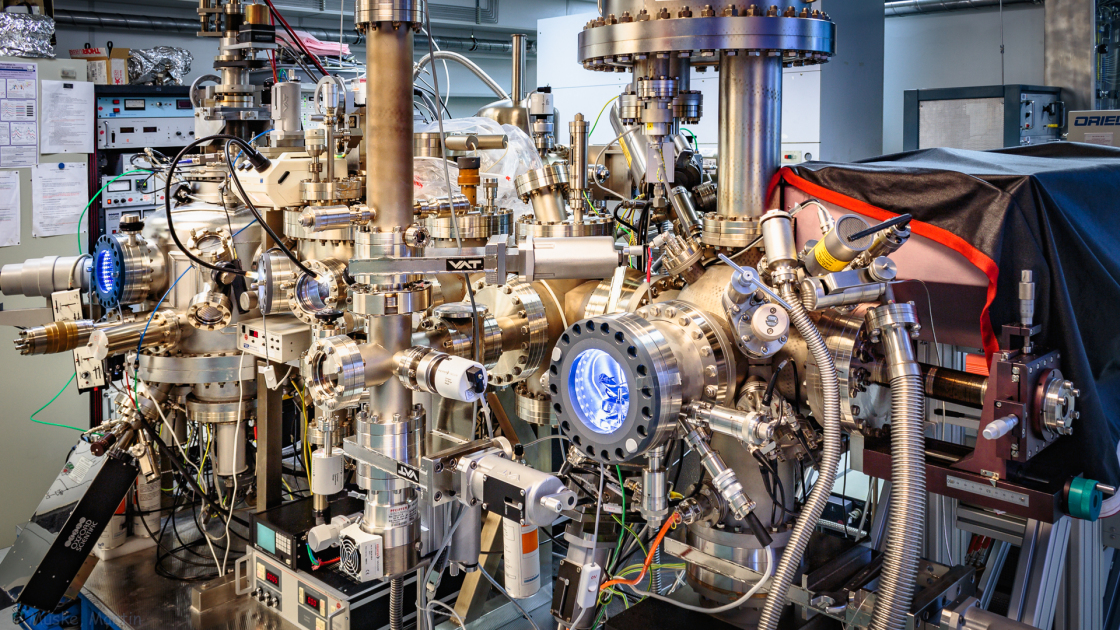
The institute Silicon Photovoltaics is operating an ultra high vacuum (UHV) tool for the preparation and characterization of semiconductor heterostructures. It is used for first, explorative investigations of novel materials that are relevant for silicon photovoltaics as well as other device concepts. The working principles, the atomic and chemical structure, and the electronic properties of heterocontact structures, their surfaces and interfaces are investigated.
Starting point for experiments in the UHV system are either 2 inch silicon wafers, or other samples with a size of up to 2.5x2.5cm². The 2" wafers are handled directly, while other samples require a sample holder. At a base pressure of ~10-10 mbar and sample temperatures up to 1050°C, solids are evaporated onto the sample by means of effusion cells and electron beam evaporators. An additional ECR plasma based atom/radical source is particularly well suited for the introduction of different gases into the layer growth. Thus, it is possible to grow oxides, nitrides and carbides under UHV base pressure conditions, as well as deposit ultra thin buffer layers of e.g. SiO, SiN, InN, or hetero emitters / charge carrier selective contacts (e.g. In2O3, In2O3/WO3 mixed oxides, etc.). The substrate surface and film growth can be monitored in situ with RHEED. In-system photoelectron spectroscopy allows for the characterization of band offsets using constant final state yield spectroscopy (CFSYS), and electronic structure and chemical bonding with X-ray and UV photoelectron spectroscopy (XPS / UPS), without breaking the vacuum. It is possible to carry out a complete in situ preparation of heterojunction solar cells with subsequent in-situ metallization (Pt, Au, Al). Furthermore, samples can be transferred in HV conditions to other systems via a dedicated transfer port.

