Öffnet in neuem Fenster
Opens in a new window
Öffnet externe Seite
Opens an external site
Öffnet externe Seite in neuem Fenster
Opens an external site in a new window
Institute Silicon Photovoltaics
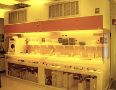
Cleanroom @EE-IS 12.8
The Institute Silicon Photovoltaics operates two clean rooms for processes of semiconductor technology based on silicon material. One of them is located in the EMIL building, the second one is situated in the EE-IS building 12.8.
This is an ISO 7 clean room where the processes mentioned below were carried out on silicon wafers and silicon layers on glass substrates, and which are mainly used for the processing of solar cells. The processible substrate sizes are between edge lenghts of 10 mm × 10 mm and 100 mm × 100 mm or diameters between 2 inch and 100 mm.
The following processes are available:
Wet-chemnistry
Laminarflow wet bench for cleaning processes
- RCA-cleaning
- H-termination of silicon surfaces
Laminarflow wet bench for etching processes
- Etching processes and structuring of different surfaces and layers such as Si, SiO2, TCO’s, metal layers (e. g. aluminum, silver)
- Photolithographic wet chemical processes (developing, etching)
- Etching of random pyramids in silicon surfaces
Fume hood with exhaust air scrubber
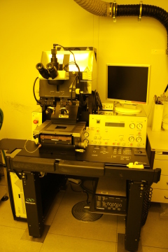
Photolithography
For photolithographic processes the following equipment is available
- spin coater for substrates up to 8 inch diameter
- Hotplate (max. 300 °C) and furnaces (max. 200 °C) for photoresist annealing
- Maskaligner MA4 and MA6 for contact exposure of substrates up to 4inch diameter or 100 mm edge length with 4 and 5 inch masks, Processing of silicon and glass substrates,Resolution up to 10 µm depending on structure and substrate
- positive and negative photoresists
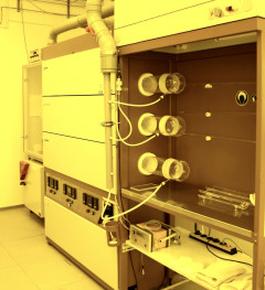
Thermal processes
High temperature processes
- dry oxidation of silicon (T≤1050°C)
- boron diffusion from source wafers (T≤ 800...1000 °C)
- Annealing in nitrogen and forming gas atmosphere (T≤ 1050 °C)
RTP-Processes
- Temperature range: 300 – 1200 °C
- inertgas atmosphere
- maximum sample size: 3 inch diameter
- heating rate 15 K/s
Metrology
-
4-point-probe for measurements of specific and sheet resistivity
-
surface profiler for measuring layer thicknesses
-
ellipsometer (IR-laser 1550 nm, VIS-laser 632 nm)
-
optical microscope (25x, 50x, 100x, 500x, 1000x), bright and dark field, camera