Institute Silicon Photovoltaics
Scanning electron microscopy (SEM)
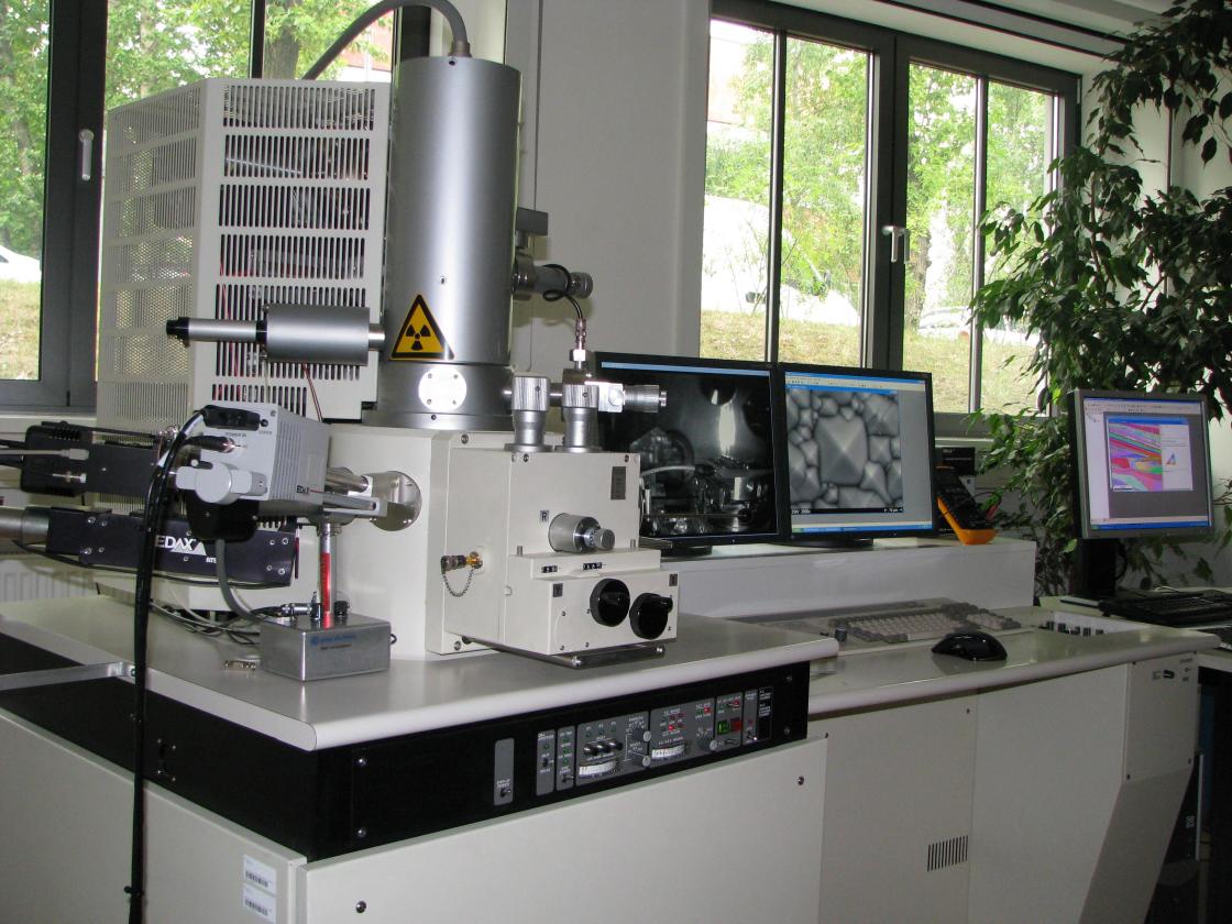
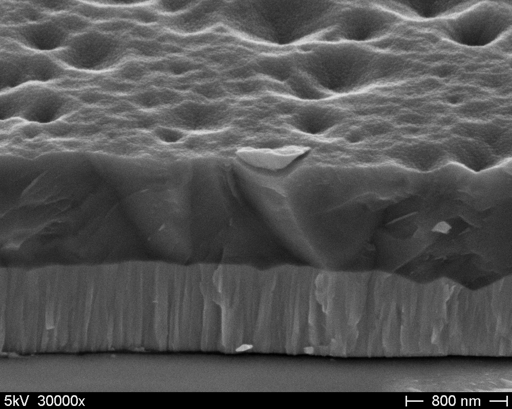
The HITACHI S-4100 scanning electron microscope (SEM) with cold field emission gun allows the investigation of the structure and surface morphology of conducting, semiconducting and insulating materials without application of conducting surface coatings. The accelerating voltage can be varied between 0.5 and 30kV. The maximum resolution is 1.5nm.
Methods
- Energy Dispersive X-ray analysis (EDX)
- Electron Backscatter Diffraction (EBSD)
- Electron Beam- Induced Current (EBIC)
Investigated materials:
- Silicon layers
- Transparent conducting oxide layers
- Ternary compound layers


