Application example
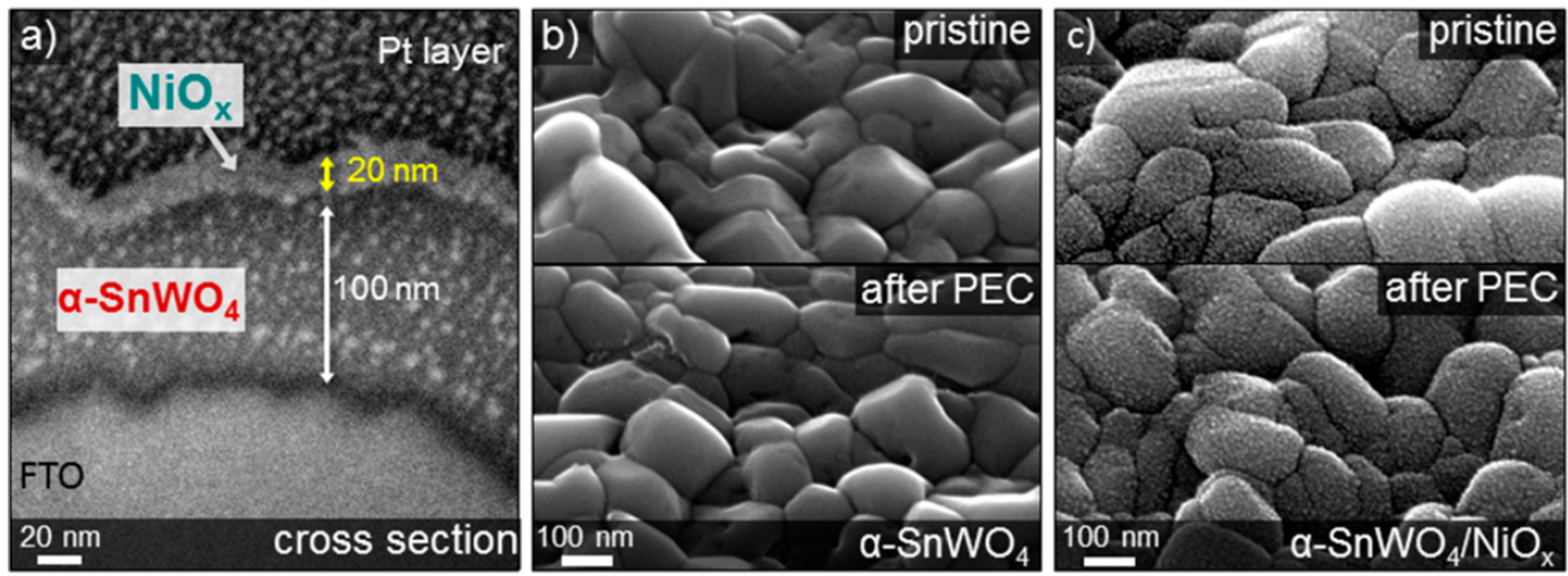
Phase-pure α-SnWO4 films were investigated as top absorber material in a tandem device for highly efficient solar water splitting. To prevent water from oxidizing the α-SnWO4, a 20 nm p-type NiOx hole conducting protection layer was deposited by pulsed laser deposition on top of the α-SnWO4. The layer is clearly visible in the FIB cross section shown in Figure 7a. Within the regions of the cross-section, the NiOx conformally covers the α-SnWO4 layer and exhibits a nanocrystalline morphology. The high-resolution SE imaging in b) and c) was performed at the Zeiss Merlin FE-SEM (also part of
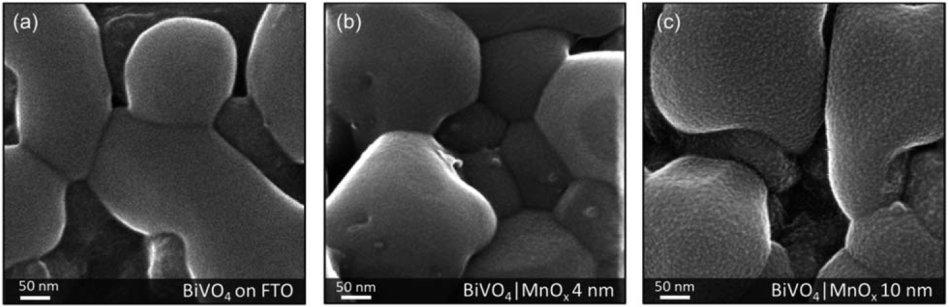
The role of atomic layer deposited MnOx co-catalysts and their thickness in the photoelectrochemical performance of BiVO4 photoanodes is investigated. The scanning helium ion microscopy top view image of the BiVO4 film shows that it is not fully compact, i.e., some parts of the FTO substrate are not covered. This confirms the presence of the pinholes, and therefore the shunting pathways decreasing the photocurrent for thicker MnOx films. (see also R. Irani, P. Plate, H. Christian, P. Bogdano, and M. Wollgarten, “The role of ultra-thin MnOx co-catalysts on the photoelectrochemical properties of BiVO4 photoanodes,” J. Mater. Chem. A 8, pp. 5508–5516, 2020.)
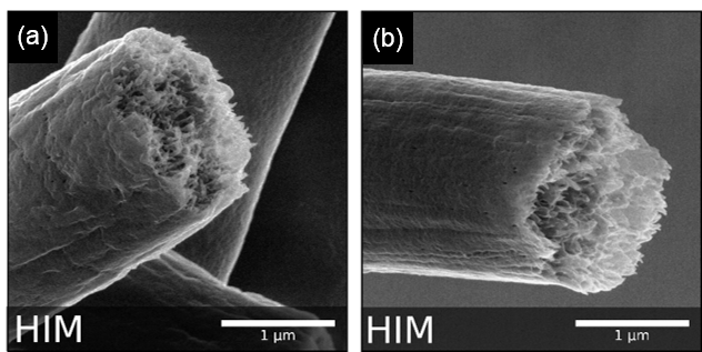
High-resolution secondary electron helium ion microscopy images of polystyrene fiber ends with different additives show the big amount of nanoscaled channels in the fiber materials and on the fiber surface. The observed morphology can be explained by the mechanism of the fiber formation during electrospinning. (see also V. Datsyuk et al., “Polystyrene nanofibers for nonwoven porous building insulation materials,” Engineering Reports 1, 12037, 2019.)
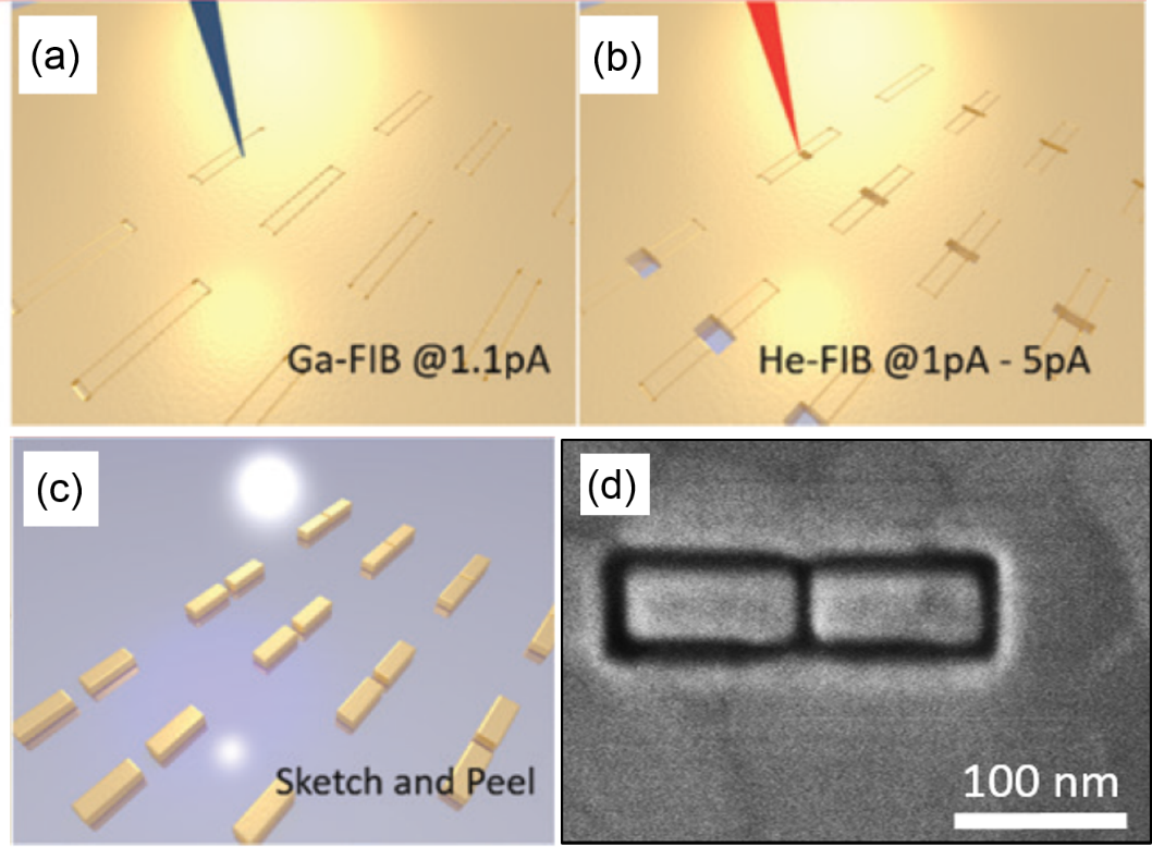
A combination of helium- and gallium-ion beam milling together with a fast and reliable sketch-and-peel technique is used to fabricate gold nanorod dimer antennas with an excellent quality factor and with gap distances of less than 6 nm.helium-ion micrograph of a prototypical antenna with a gap size of 5 nm is displayed, in which the high uniformity of the gap region becomes visible. (see also M. Gittinger, K. Höflich, V. Smirnov, H. Kollmann, and C. Lienau, “Strongly coupled , high-quality plasmonic dimer antennas fabricated using a sketch-and-peel technique,” Nanophotonics 9 (2), 401, 2020.)