Institute Silicon Photovoltaics
Hetero-junction solar cells based on a-Si:H / c-Si (HETSI)
EU-Projekt (2008- 2011)
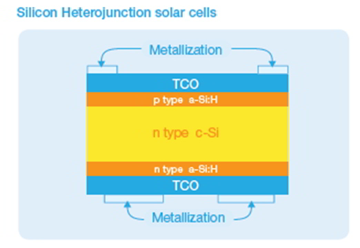
Within the HETSI ( Hetero-junction solar cells based on a-Si:H / c-Si ) project, funded by the European Union in its 7th framework program under grant no. 211821, the use of amorphous/crystalline (a‑Si:H/c‑Si) heterojunctions for wafer-based high-efficiency solar cells is investigated. The heterojunction concept is a promising option to reach very high efficiencies and high throughput for wafer based crystalline silicon technology. Main objectives are to reach up to 21% power conversion efficiency on large area monocrystalline silicon thin wafers and to be able to develop a suitable cell and module process at the industrial level. Another important objective is to prove that this technology can be cost effective. Finally a long term concept is evaluated with an innovative structure that uses a‑Si:H/c‑Si heterojunctions for rear contact cells.

Project partners:
- INES - French National Institute For Solar Energy
- CNRS - French National Research Center, labs LGEP-Supélec
- and LPICM
- ECN - Energy Research Centre of the Netherlands
- ENEA - Italian National agency for new technologies, Energy and sustainable economic development
- IMEC - Interuniversity Microelectronic Centre
- EPFL-IMT Ecole Polytechnique Fédérale de Lausanne IMT Neuchâtel
- University Utrecht
- Photowatt
- Q-Cells SE
- Solon
- ALMA Consulting Group
Within HETSI, HZB has focused on
- the development and characterization of contact layers (a-Si:H, µc-Si:H, TCO)
- improving the understanding of interface and device physics using novel characterization tools (e.g. Near-UV PES and simulation)
- further development of HZBs device simulator AFORS-HET
- processing of proof-of-concept small size (typ. 1cm²) solar cells, both of the conventional type with contacts on front and back side as well as rear contact cells
