Institute Silicon Photovoltaics
a-Si/c-Si-hetero solar cells
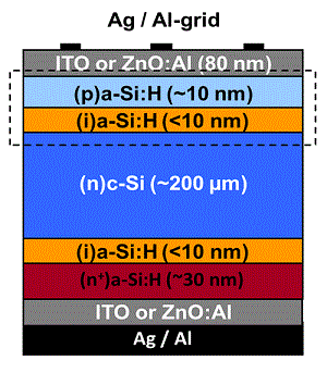
We aim at developing efficient amorphous/crystalline silicon heterojunction solar cells (Fig. 1), in close collaboration with HZB's institute PVcomB. Monocrystalline silicon wafers (c-Si) and thin polycrystalline silicon absorbers on glass are used as substrates to absorb the sunlight. Thin amorphous silicon (a-Si:H) films are deposited onto the substrate using plasma-enhanced chemical gas phase deposition (PECVD) to form the solar cell's emitter and back surface field (BSF). Alternatively, nanocrystalline (nc-Si:H) or oxidic (a-SiOx:H) films are available by changing the plasma parameters. The TCO (Transparent Conducting Oxide) provides a conductive path towards the metal grid fingers. It is deposited onto the amorphous emitter and BSF films using magnetron sputtering.
The difference between this technology and conventional solar cell preparation is that no high temperature diffusion processes are needed any more. The whole solar cell is processed at temperatures below 250°C. Furthermore, the excellent passivation of the c-Si surface by a-Si:H yields the potential for very high open circuit voltages (Voc >> 700 mV), thus for high efficiency solar cells [1].
The interface between a-Si:H and c-Si has a major impact on the cell’s Voc and thus on the cell efficiency. Chemical pre-processing of the wafer and amorphous silicon deposition conditions have to be optimized in order to minimize the a-Si:H/c-Si interface density of states.
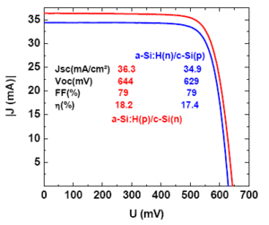
Fig. 2 shows the I-V curves under AM1.5 illumination of such a-Si:H(n)/c-Si(p)- and a-Si:H(p)/c-Si(n) solar cells. The efficiencies are the highest published for a direct heterojunction between c-Si wafer and doped amorphous silicon. However, the defect density in doped amorphous silicon limits the Voc in this case.
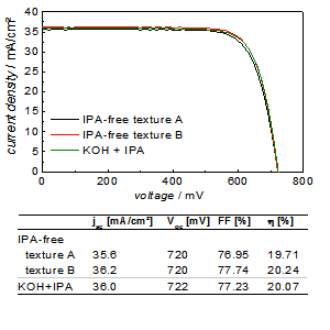
If additional undoped (i)aSi:H buffer layers of a few nanometers thickness are inserted in the junction, Vocs far above 700 mV are possible.
Fig. 3 shows an example for cells with (i)a-Si:H buffer layers [3].
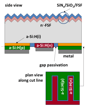
Further improvements of cell efficiency are possible if both contacts of the cell are moved to the rear side of the wafer (Fig. 4): shadowing and parasitic absorption losses at the front grid and in the TCO/a-Si:H stack, respectively, are eliminated in such rear contact cells and the photocurrent increases.
Currently, HZB achieves such heterojunction solar cells with an interdigitated back contact (IBC) at efficiencies above 22% [4,5].
References
[1] W. G. J. H. M. van Sark, L. Korte & F. Roca (Eds.): Physics and Technology of Amorphous-Crystalline Heterostructure Silicon Solar Cells. Springer (2011).
[2] L. Korte; E. Conrad; H. Angermann; R. Stangl & M. Schmidt: Advances in a-Si:H/c-Si Heterojunction Solar Cell Fabrication and Characterization. Sol. En. Mat. Sol. Cells 93 (2009) 905-10.
[3] Jan Kegel, Heike Angermann, Uta Stürzebecher, Erhard Conrad, Mathias Mews, Lars Korte, Bert Stegemann: Over 20% conversion efficiency on silicon heterojunction solar cells by IPA-free substrate texturization. Applied Surface Science 301 (214) 56–62.
[4] J.-C. Stang, T. Franssen, J. Haschke, M. Mews, A. Merkle, R. Peibst, B. Rech, and L. Korte: Optimized Metallization for Interdigitated Back Contact Silicon Heterojunction Solar Cells. Solar RRL 1 (2017) 1700021.
[5] J.-C. Stang, J. Haschke, M. Mews, A. Merkle, R. Peibst, B. Rech, and L. Korte: Aluminium metallisation for interdigitated back-contact silicon heterojunction solar cells. Jap. Journal of Applied Physics 56 (2017) 08MB22.


