Institute Silicon Photovoltaics
Silicon based Heterostructures
Heterostructures represent a basic structure in solid state physics and electronic devices (field effect transistors, III-V semiconductor based optoelectronics, solar cells).
They allow:
- To combine the mostsuitable properties of different solids
- Passivation of interface states
- To build bridges between organic and inorganic solids
Our research activities focus on the amorphous/crystalline silicon (a-Si:H/c-Si) heterojunction.
Fig. 2 shows the schematics and band structure of a wafer-based solar cell with a-Si:H/c-Si heterocontacts. The use of amorphous silicon deposition instead of in-diffusion of dopants makes it possible to form a p-n heterojunction and, at the same time, maintain a well passivated c-Si surface.
Chemical vapour deposition of a-Si:H and sputter-deposition of a transparent conductive oxide (TCO) front contact at low temperatures (T<250°C) enables the realization of a complete low temperature processing on thin poly-crystalline silicon films on glass or on silicon wafers for high efficiency hetero-solar cells. Cell efficiencies above 25 % on large area (100 cm²) have been shown for a "classical" cell design with contacts on the front and rear side.
A crucial pre-condition to avoid recombination losses of charge carriers on hetero-interfaces is the optimisation of wet-chemical conditioning of Si substrates for heterojunction solar cells.
Further improvements are possible using alternative designs such as rear contact cells, as shown experimentally and in numerical simulation studies using e.g. our heterojunction device simulator AFORS-HET.
Another topic of current research is to combine silicon heterojunction with perovskite-based solar cells into perovskite/silicon tandem cells. With realistic assumptions regarding the involved materials, numerical simulations predict efficiencies above 30% for such devices.
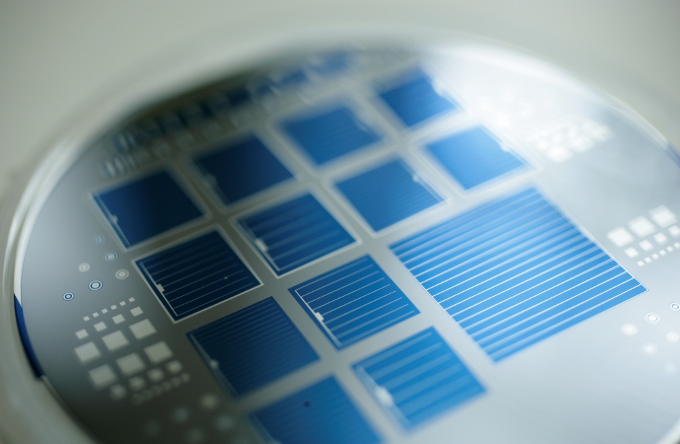
Fig. 1 Photo of a silicon wafer with a-Si:H/c-Si wafer solar cells, processed at HZB
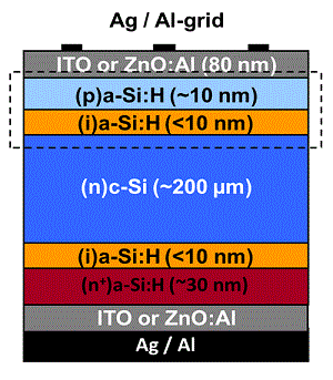
Fig. 2a Structure of a (wafer-based) amorphous/crystalline heterojunction solar cell. For clarity, the usual surface texturization is omitted.
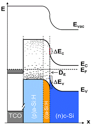
Fig. 2b Band structure of the TCO/(p,i)a-Si:H/(n)c-Si-heterojunction. ΔEV, ΔEC are the band offsets at the heterocontact, Dit denotes interface defects.