Institute Silicon Photovoltaics
Surface Photovoltage
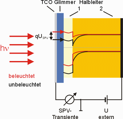
The surface photovoltage technique utilizes the change of the electrochemical potential in the space-charge region(s) of a semiconductor during excess carrier generation due to illumination of the sample with light of suitable wavelength and intensity.
The sample that is to be examined is placed in an artificial metal-insulator-semiconductor (MIS) structure so that the change in surface photovoltage can be measured as a transient in the external circuit. There is no need for any time consuming contact preparation on the samples, making the SPV method suitable for quick sample characterization.
According to the experimental conditions, the SPV method allows the analysis of a multitude of different semiconductor parameters, such as carrier lifetime, band bending and the density of interface states.
Dynamic SPV
In the dynamic SPV method the sample is illuminated by a monochromatic light pulse with high intensity.
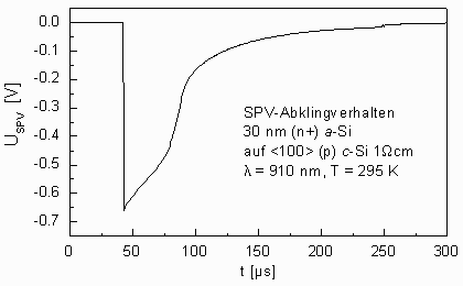
In dependence on the length of the excitation pulse (pulse length dependent SPV, PD-SPV) and on the photon flux (intensity dependent SPV, ID-SPV) the recorded SPV transients allow statements on the surface band bending, the recombination behaviour and the excess carrier lifetime. If one uses an external bias voltage (voltage-dependent SPV, VD-SPV) an examination of the energetic distribution of interface states (Dit) is possible.
Static SPV
In the static SPV method the sample is illuminated with monochromatic light and tuneable wavelength. So the penetration depth of the photons in the sample can be changed. The measured photovoltage is kept constant at each wavelength by adjusting the light intensity. These parameters allow statements on the diffusion length of the excess carriers in the sample.
Equipment
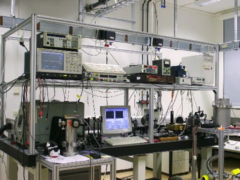
Si-Photovoltaics operates several SPV setups, each optimized to the demands of the special experimental task. All setups are equipped with high input resistance, low capacity buffer amplifiers and allow the measurement of the MIS capacity.
SPV setups for quick sample characterization utilize semiconductor laser diodes for measurements at room temperature λ=910 nm, PLaser=210 W, tLaser=160 ns) and temperatures down to 90 K (λ=905 nm, PLaser=150 W, tLaser=100 ns).
Deeper insights in the physics of the SPV method are possible with a setup equipped with a Nd:YAG laser system and optical parametrical Oscillator ((λ=400 ...2500 nm, ELaser= 50 J, tLaser=5 ns) as well as with a semiconductor laser (λ=910 nm, PLaser=18 W (CW), tLaser=100 ns - CW).
Its possible to measure at room temperature as well as at temperatures down to 90 K with this setup. SPV and photoluminescence can be measured at the same time, too.
Material systems that have been characterized:
c-Si: density of surface states Dit in dependence of the chemical pre-treatment of the sample, effective carrier lifetime, effective diffusion length
SiO2/c-Si: density of interface states, effective carrier lifetime
a-Si/c-Si: c-Si band bending at the interface, density of interface states, effective carrier lifetime in dependence of the a-Si deposition parameters


