Department Microstructure and Residual Stress Analysis
Real-time Analysis of Energy Materials
Detailed insights into the reaction processes during the formation or degradation of thin film compound semiconductors are gained by synchrotron-based in situ and real-time X-ray diffraction and fluorescence analysis (XRD/XRF) in combination with numerical modeling. A high-brilliance metal-jet X-ray source enables time resolutions in the second and subsecond regime in the laboratory, which were previously only possible at synchrotron beamlines. The understanding of the complex reactions taking place during thin film deposition or battery cycling is essential for the improvement of existing as well as for the development of novel solar cell and battery concepts.
Mapping the temperature range of Caesium-based inorganic halide perovskites
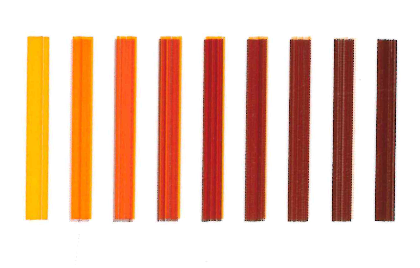
Nine samples with mixtures from CsPbBr2I (ink 1, left) to pure CsPbI3 (ink 2 right). © H. Näsström/HZB
For novel multi-component material, analyzing the crystalline phases in a wide temperature and composition range is usually a tedious and time-consuming task. This demonstrates how the work load for such a study can be significantly reduced by using a lab-based high-brilliance X-ray source. Stripes with varying composition were printed onto a substrate. During a single heating process, the phases of the different compositions were sequentially analyzed for each temperature by moving the sample in the direction perpendicular to the stripes. Thanks to the high photon flux of the metal-jet X-ray source, each XRD measurement only took 10 seconds. With this approach, the phase transitions for CsPb(I1-xBrx)3 with variation of x and in the temperature range from room temperature up to 300 °C for both heating and cooling could be analyzed within a few hours.
Näsström, P. Becker, J. Márquez, O. Shargaieva, R. Mainz, E. Unger and T. Unold. Dependence of Phase Transitions on Halide Ratio in Inorganic CsPb(BrxI1-x)3 Perovskite Thin Films Obtained from High-Throughput Experimentation. J. Mater. Chem. A (2020), doi: 10.1039/D0TA08067E.
Defect annihilation in compound semiconductor films

The upper graph show real-time X-ray diffraction intensities during deposition of Cu-Se onto a Cu(In,Ga)Se2 film, showing the disappearance of a typical planar defect signal. The lower graph shows electron microscopy images of a film before (left) and after (right) defect annihilation.
A major problem of compound thin-film solar cells, such as Cu(In,Ga)Se2, is the large gap between lab efficiencies and commercial module efficiencies. A large process parameter space makes trial-and-error optimization a time-consuming and expensive task. Therefore, understanding the underlying atomic-scale physics and chemistry is essential to identify the potential origins of efficiency losses in the transfer from lab- to large-scale fabrication. In this contribution we present results from an international collaboration that provides direct insight into defect formation and annihilation during the fabrication of Cu(In,Ga)Se2 films. Real-time X-ray diffraction reveals that these faults are nearly completely annihilated during an intermediate Cu-rich process stage.
Mainz, E. Simsek Sanli, H. Stange, D. Azulay, S. Brunken, D. Greiner, S. Hajaj, M. D. Heinemann, C. A. Kaufmann, M. Klaus, Q. M. Ramasse, H. Rodriguez-Alvarez, A. Weber, I. Balberg, O. Millo, P. A. van Aken and D. Abou-Ras. Energy Environ. Science 9, 1818-1827 (2016), doi: 10.1039/c6ee00402d.
Grain growth driven by a metastable-to-stable phase transition from wurtzite nanorods to large grained kesterite films
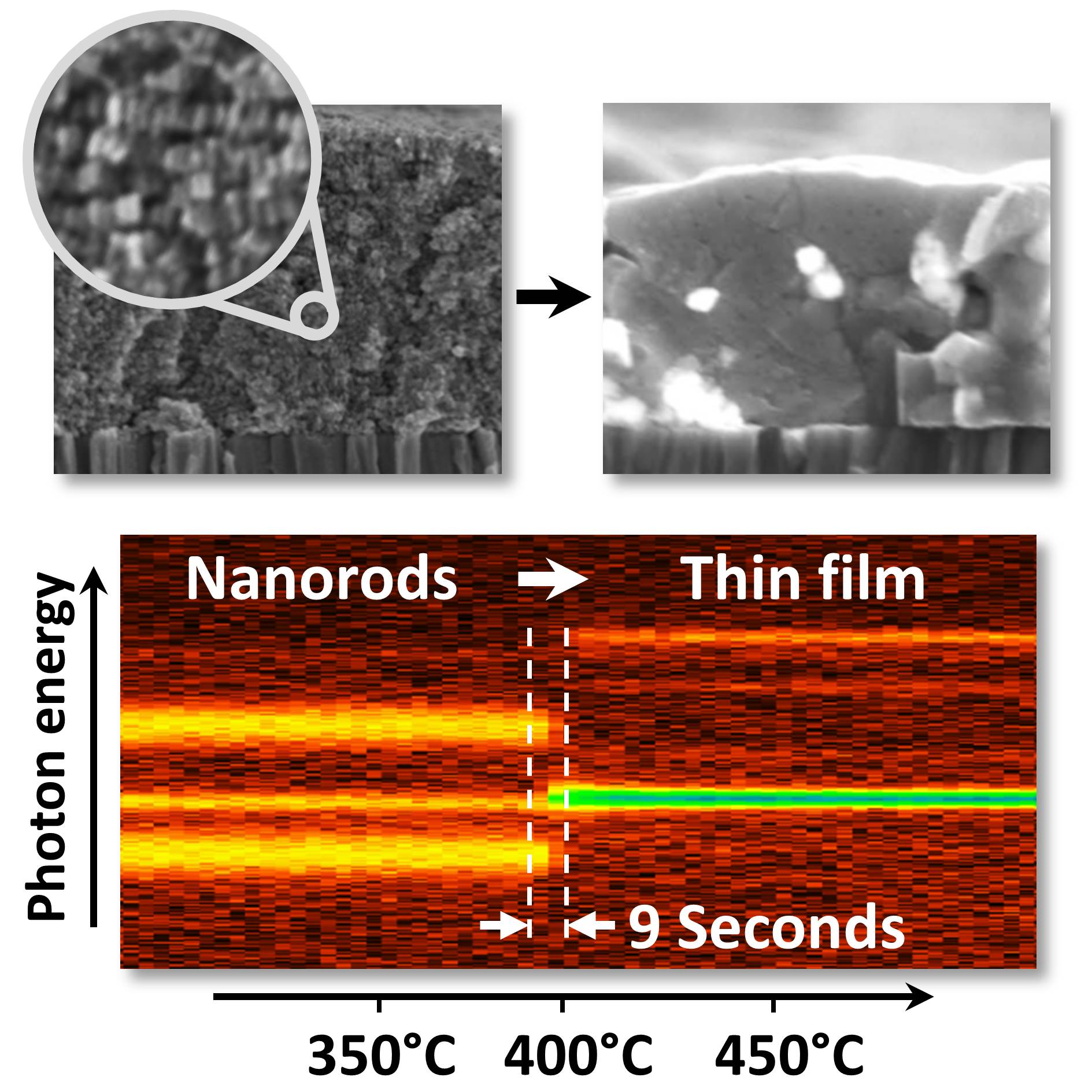
The transformation from a layer of closely packed nanorods (top left) to a polycrystalline semiconductor thin film (top right) could be observed in by in-situ X-ray diffraction in real time (bottom). A detailed analysis of the real-time signals reveals that the transformation of the nanorods into kesterite crystals takes only 9 to 18 seconds.
The driving force for grain growth in compound semiconductors is often rather week and hence the growth is slow and needs high temperatures. However, this limitation can be overcome by a little trick: Instead of depositing material directly in its desired structure, it is deposited in the form of nanorods, in which the atoms are arranged in a slightly different, metastable way. We found that in this case, the growth of new grains is directly connected with a phase transition from the instable phase of the nanorods to the stable phase of the growing kesterite grains. During this phase transition, the chemical composition does not change. Thus, on the one hand there is an increased driving force for the grain growth caused by the phase transition, while on the other hand the atoms do not have to move much. The combination of both is - according to our model - what lets the grains grow very fast, even at comparably low temperatures.
R. Mainz, A. Singh, S. Levcenko, M. Klaus, C. Genzel, K. M. Ryan and T. Unold. Nature Communications 5, 3133 (2014), doi: 10.1038/ncomms4133.
Press release
Phase formation and structural defect annihilation during coevaporation of Cu(In,Ga)Se2 absorber films
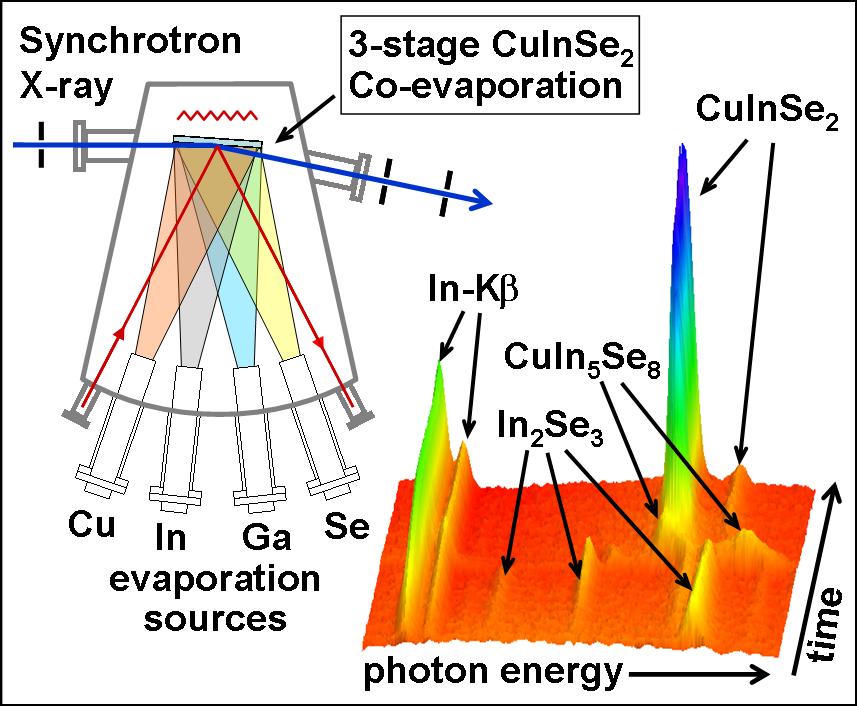
Polycrystalline film growth during coevaporation observed in real time using in situ X-ray diffraction and fluorescence analysis.
Highest thin film solar cell efficiencies are gained on the basis of Cu(In,Ga)Se2 absorbers synthesized by coevaporation. For the first time the formation of crystalline phases during such growth processes could be analyzed in real time. To achieve this goal a novel in situ coevaporation chamber was deleveloped in collaboration with the group of Dr. Christian Kaufmann. The chamber is taylor-made for operation at the Berlin electron storage ring BESSY II. Our first results provide new insights into the phase formation and segregation of secondary Cu-Se phases and their direct correlation with defect annihilation. By means of model calculations of the fluorescence signals, we observe that secondary Cu2Se penetrates into the CuInSe2 film, whereas in the case of CuGaSe2 it remains at the surface of the film.
H. Rodriguez-Alvarez, A. Weber, J. Lauche, C. A. Kaufmann, T. Rissom, D. Greiner, M. Klaus, T. Unold, C. Genzel, H.-W. Schock and R. Mainz. Advanced Energy Materials 3, 1381-1387 (2013), doi: 10.1002/aenm.201300339.
Cu2ZnSn(S,Se)4 film formation from nanoparticles
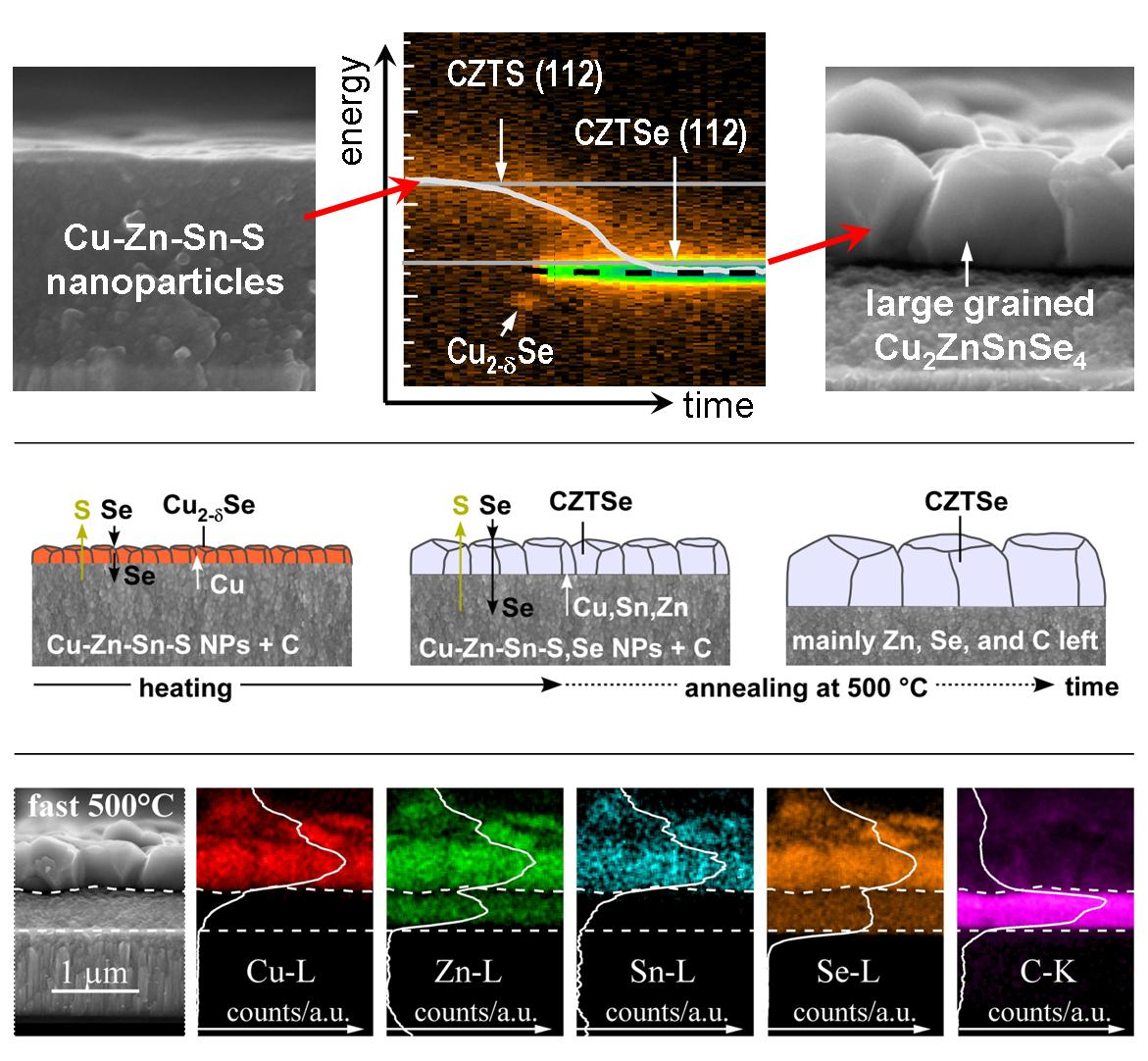
Real-time diffraction and fluorescence analysis reveals that during selenization of Cu-Zn-Sn-S nanoparticle precursor films, cations diffuse out of the nanoparticle layer to form large Cu2ZnSnSe4 grains at the surface through a self-controlled reaction via an intermediate Cu-rich growth. (c) RSC
A synthesis route via nanocrystal precursors deposited as ink has the potential to replace expensive vacuum-based deposition of compound semiconductor absorber films. The use of earth-abundant elements and low energy consumption turns this approach into a promising candidate for sustainable and low-cost solar module fabrication. For the first time we studied the reaction path and grain formation during such a process in real time. Surprisingly, we found that large grains form by cations that diffuse out of the nanoparticle layer to the surface of the film instead of a growth of the nanocrystals. This leads to a self-controlled reaction via an intermediate Cu-rich stage and explains the high crystal quality of the resulting absorber layer as well as the accumulation of remaining carbon at the bottom of the film.
R. Mainz, B. Walker, S. S. Schmidt, O. Zander, A. Weber, H. Rodriguez-Alvarez, J. Just, M. Klaus, R. Agrawal and T. Unold. Phys. Chem. Chem. Phys. 15, 18281-18289 (2013), doi: 10.1039/C3CP53373E.
Modeling of depth distributions from Bragg and fluorescence signals
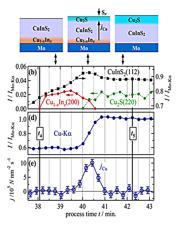
Real-time observation of Cu diffusion through CuInS2 during film growth. (c) AIP
During film formation, the depth distributions of the involved elements undergo constant changes. We developed a combined evaluation of in situ recorded diffraction and fluorescence signals to extract time-resolved elemental depth distributions during film growth. The graph shows a series of depth distributions obtained by this method during the growth of CuInS2. The CuInS2 layer forms on top of the metal layer. After all indium is consumed for the formation of CuInS2, the excess Cu quickly diffuses through the chalcopyrite layer to form Cu2S at the surface. We propose that this procedure plays an important role for the quality of the material.
R. Mainz and R. Klenk. J. Appl. Phys. 109, 123515 (2011), doi: 10.1063/1.3592288.