Department Structure and Dynamics of Energy Materials
Instrumentation and Laboratory
Instrumentation at BESSY II
| Instrument | Contact | |
|---|---|---|
| Diffraction@KMC-2 | Diffraction /KMC-2 | Daniel Többens |
| mySpot | Micro-XANES, -EXAFS, -fluorescence, -SAXS, -WAXS, -Raman Scattering /7T-WLS-1 | Ivo Zizak
Ana Guilherme Buzanich |
| XANES@KMC-2 | XANES@KMC-2 | Götz Schuck |
X-Ray CoreLab

The laboratory operates instruments for various X-Ray diffraction methods at HZB locations Adlershof (WCR) and Wannsee (LMC) and makes them available to all interested co-workers of HZB as well as for guests.
Laboratory for crystallographic materials research for solar energy conversion
- synthesis of powder reference samples of chalcogenide compound semiconductors by solid state reaction (fig. 1)
- synthesis of single crystals of novel PV materials (fig.2)
- synthesis of hybrid-perovskites
- chemical analysis of the synthesized material by WDX spectroscopy using an electron microprobe system
(Freie Universitaet Berlin, Institute of Geological Sciences) - basic structural analysis of the synthesized materials by X-ray powder diffraction
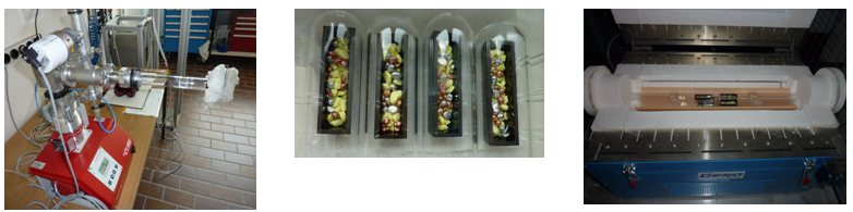
Fig. 1: left: sealing of evacuated silica tubes; middle: elements loaded into a graphite boat within a silica tube; right: synthesis in a 1-zone furnace
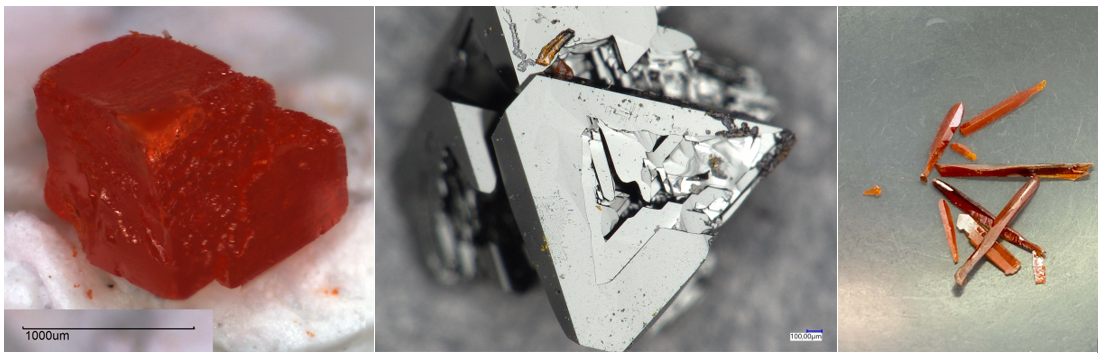
Fig. 2: MAPbBr3 single crystals, grown from solution (left) and defect adamantine CuAlSnS4 (center) and CuGaGeS4, both grown by chemical vapour transport (CVT)
UV-Vis laboratory
At the UV-Vis laboratory, diffuse reflectance spectroscopy measurements in the ultra-violet and visible spectrum are done. For this a Perkin Elmer Lambda 750S equipped with a “praying mantis” stage, specifically designed for the measurements of powders with low signal is available, with sample holders for small and very small amounts of powder.
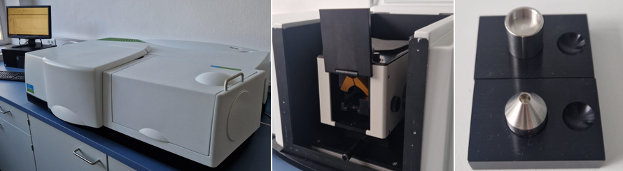
Figures: Perkin Elmer Lambda 750S (left), "Praying mantis" stage (center), two types of powder holders (right)
Optical Microscopy
A modern optical microscope Keyence VHX970 with Objective ZS 20 x 100 is mostly used for the selection of individual high-quality single crystals suitable for further analysis.
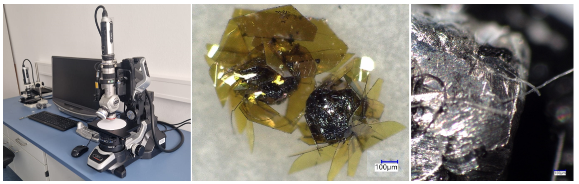
Figure: Optical microscope Keyence VHX970 (left), Ag2FeSnS4 surrounded by SnS2 single crystals (center), Sb2Se3 polycrystalline bulk (right)
ESMI - Electronic Structure of Materials and Interfaces

At the ESMI laboratory we focus on the advancement of facile methods for high-throughput and reliable characterization of materials surface and interface electronics for modelling and development of new effective optoelectronic devices. Kelvin probe (KP) and photoelectron yield spectroscopy (PYS) are key methods for investigation of the electronic structure of materials and interfaces, e.g., work function (WF) and related Fermi level position, ionization energy (IE) and related valence band maximum, defect states and their distribution by energy. In contrast to similar methods developed for studies in ultra-high vacuum (UHV), the KP and PYS in our ESMI lab are combined for studies at ambient pressure under inert gases (N2 or Ar).
SEM laboratory
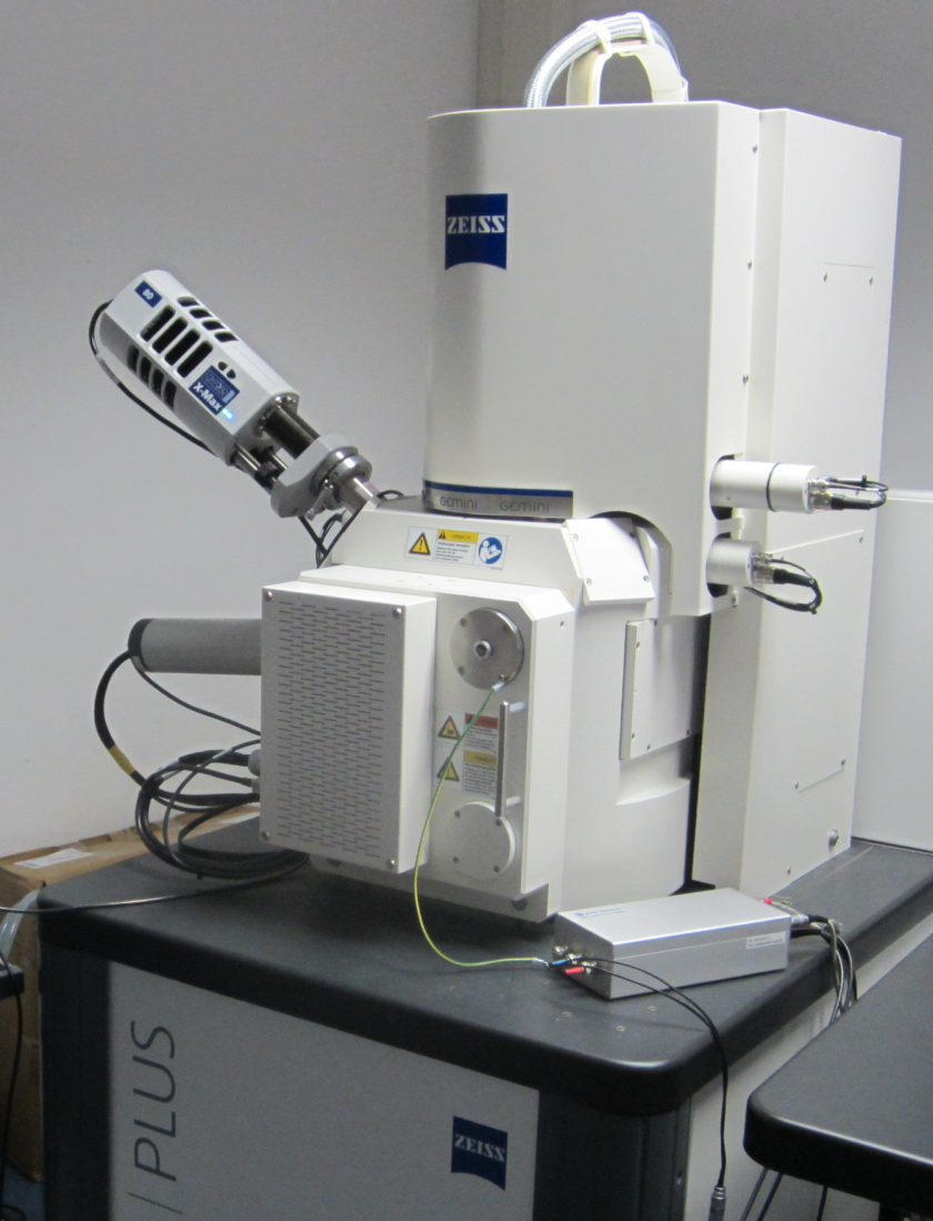
In the SEM laboratory, we operate scanning electron microscopes (Zeiss UltraPlus und LEO GEMINI 1530) for the analysis of materials and devices used in photovoltaics, for solar-fuel production, catalysis, batteries, as well as quantum materials, superconductors, etc. We apply an extensive range of methods comprising imaging, energy-dispersive X-ray spectroscopy (EDXS), electron backscatter diffraction (EBSD), cathodoluminescence (CL), and electron-beam-induced current (EBIC) measurements. Moreover, specimens for SEM and TEM analyses can be prepared in the corresponding preparation lab equipped with highly specialized instrumentation.
The SEM laboratory and sample preparation participate in the CoreLab CCMS.