Department Optics for Solar Energy
Methods
Nanoimprint lithography
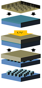
Fig. 1 Illustrating the replication process using a PDMS stamp.
Nanoimprint Lithography (NIL) is a surface patterning technique first introduced in 1996 by Prof. Stephen Chou and his colleagues [1,2]. This new technology had such an important impact in so many research fields that it has been listed in 2003 by the Massachusetts Institute of Technology as one of 10 emerging technologies that will strongly impact the world [3]. Indeed beside its ultrahigh resolution reproduction capability (up to 5 nm) this technology is also very cost effective, easy to process and therefore makes it a serious candidate for the implementation of up-scaling applications and large scale industrial fabrication.
The principle of NIL (sometimes also called “hot embossing”) is very simple. A template or mold (e.g. a silicon wafer textured with nanoscale features) is pressed with a controlled pressure and temperature onto a substrate coated with a defined layer of polymeric material. After the mold removal an inverse reproduction of the features will then be directly imprinted onto the substrate. Recently new UV-curable polymer materials (also called resists) have appeared on the market and have been used for nanoimprinting technology. This UV-NIL process makes it even simpler and faster than the traditional hot embossing technique because it can be done at room temperature. The only requirement is then to have a transparent mold which allows the UV light to pass through for the curing of the resist. The most common process is to make first a so-called transparent stamp of the original template and then use this stamp for the replication process of the resist dispersed onto the substrate. Poly(dimethyl siloxane) block polymer (PDMS) is commonly used for the fabrication of the transparent stamp. This material offers a very high resolution patterning and is also easy to separate from the mold due to its low surface energy.

Fig 2 PDMS stamp replication of three fields (6x8 mm2) with a hexagonal lattice structure with periods ranging from 600 to 800 nanometers.
In our department, we use UV-NIL technology to produce nanostructured glass substrates. These are coated with a UV-curing hybrid polymer, which is textured using a PDMS stamp. This method gives us a high degree of control and flexibility when texturing the glass substrates, for example with regard to the period, the aspect ratio or the height of the structure to be transferred. These textures have various functions in the development of new types of solar cells and are used, among other things, for improved light capture and better wetting.
Literature
- Chou, S.Y.; Krauss, P.R.; Renstrom, P.J.: Imprint Lithography with 25-Nanometer Resolution SCIENCE 5. april 1996 Vol 5258, pages 85-87. DOI: 10.1126/science.272.5258.85
- Chou, S. Y.; Krauss, P. R.; Renstrom, P. J.: Nanoimprint lithography. J. Vac. Sci. Technol. B 14(6), 4129 (1996) DOI: https://doi.org/10.1116/1.588605
- MIT Technology review, Feb. 2003
Hot Embossing

Our hot Embosssing-Press setup. Picture Sarah Liedtke/HZB
Hot embossing is a replication technique used for transferring micro- and nanostructures from a patterned mold onto thermoplastic polymer substrates, such as polyethylene terephthalate (PET), Polycarbonate(PC), Ethylene-Tetrafluoroethylene (ETFE), Ethylene-Tetrafluorethylene-Copolymer (ETFCE). The process uses a combination of heat and pressure to structure the polymer according to the mold features.
The hot embossing process begins by heating the polymer to a specific embossing temperature, which lies between its glass transition temperature and melting temperature. During the heating phase, the mold is already in contact with the polymer, and pressure is applied. Once the embossing temperature is reached, the main structuring phase occurs, where the temperature and pressure are held constant for a defined embossing time to allow accurate pattern transfer. After this process, the polymer is cooled below its glass transition temperature while still under pressure. Once the material has sufficiently cooled, the pressure is gradually released, and the mold is separated from the embossed substrate.
To ensure high replication fidelity and structural accuracy, several key parameters must be optimized based on the specific material and application, including the embossing temperature, embossing pressure and demolding temperature.
Compared to other structuring techniques such as photolithography or etching, hot embossing provides high-resolution replication with relatively low costs and simple techniques. However, it suffers from slow cycle times, mold wear, and challenges in thermal control and alignment.
Optical simulations
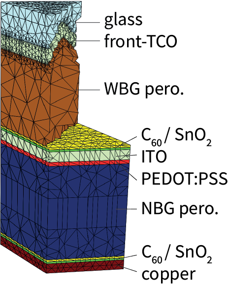
Figure: Layer stack of a nanotextured all-perovskite tandem solar cell. The figure shows the grid that is used in the simulations with the finite element method. The layers are glass, a transparent conducting oxide (TCO) as electric front contact, a self-assembled monolayer as hole-conducting layer (omitted in the optical simulations), wide-bandgap (WBG) perovskite, the electron transport layer (ETL) consisting of C60 and tin oxide (SnO2), indium tin oxide (ITO) recombination layer, PEDOT:PSS as hole-conducting layer of the bottom cell, narrow-bandgap (NBG) perovskite, ETL consisting of C60 and SnO2, and a copper back contact [2].
For high-performance, solar cells must absorb as much of the incoming light as possible. Optical simulations help to design solar cells such that they minimize reflective losses and absorption in layers, where the absorbed photon energy cannot be utilized.
Planar solar cells (without textured interfaces) can be treated with 1-dimensional analytical models such as the transfer matrix method or the net radiation method, but the partially coherent nature of the sunlight must be considered. Usually this is done by deciding a priori, in which (thick and thin) layers propagation of light should be treated incoherently or coherently, respectively. At SE-AOPT we have been using the software package GenPro4 by Delft University of Technology [1] for this kind of simulations for many years.
Silicon solar cells usually have micrometer-sized quasi-random pyramids at their interfaces. Because of their size interaction of light with the pyramids usually is treated with geometrical optics, e.g. with ray tracing approaches. Also, for these simulations, we have been using GenPro4.
Device designs with periodically structured interfaces, which we can manufacture with nanoimprint lithography, can be treated with rigorous Maxwell solvers, e.g. using the finite element method. For these simulations, we have been closely collaborating with the Computational Nano Optics group at Zuse Institute Berlin and their spinoff company JCMwave GmbH. The Department Optics for Solar Energy is a founding partner of the Berlin Joint Lab for Optical Simulations for Energy Research (BerOSE) which was founded by HZB, ZIB and the Free University Berlin in 2014. BerOSE forms an ideal environment for the interaction between experts in 3D optical computation and scientists in the synthesis of nanostructured materials for solar electricity generation, energy storage and photonics.
Literature
[1] R. Santbergen, T. Meguro, T. Suezaki, G. Koizumi, K. Yamamoto, and M. Zeman, IEEE J. Photovolt. 7, 919 (2017).
[2] K. Jäger, A. Tejada, S. Berwig, M. Hammerschmidt, P. Tockhorn, S. Albrecht, and C. Becker, Advanced Theory and Simulations 8, 2400724 (2024).