Institute Solar Fuels
Thin film deposition
Atomic layer deposition (ALD) for solar fuels
Research expertise
Three efficiency loss processes can be identified in photoelectrochemical cells:
- Poor stability: the performance of semiconductor photoelectrodes degrades over time due to corrosion of the photoelectrode material.
- Poor catalytic activity: Slow charge kinetics at the electrode/electrolyte interface limits the hydrogen (oxygen) production efficiency.
- Bulk recombination: Photo-generated charge carriers recombine before reaching the back contact or electrolyte.
A solution would be to protect the semiconductor with a corrosion protection layer, enhance the catalytic activity with a catalyst, and reduce the path length of the charge carriers by adopting nanostructured photoelectrode configurations.
Since photoelectrodes have a very large specific surface area, due to a high porosity or nanostructuring, a deposition technique is required that can conformally coat these surfaces. Additionally, this technique should be able to deposit thin films (1 - 5 nm), since thin films are necessary to allow for charge transport, minimize parasitic light absorption, and/or reduce the path length of the charge carriers. Atomic layer deposition is such a technique.
Atomic layer deposition is a vapor-phase deposition technique in which thin films are prepared sub-monolayer by sub-monolayer by repeating two subsequently executed half cycles (Fig. 1). The surface reactions are self-limiting, which leads to excellent growth control (atomic layer precision), uniform deposition over large areas, and conformal deposition in high aspect ratio substrates.
Currently, we focus on three research topics.
- Understanding the charge transport mechanism in corrosion protection layers. (TiO2, GaOx)
- Understanding the role of the catalyst (MnOx, NiOx)
- Development of new ALD processes for novel ternary metal oxides. (BiVO4, TaONx)
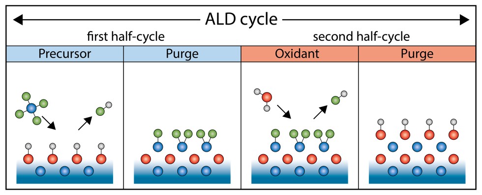
Fig. 1
thermal ALD: Home-build thermal ALD system connected to an UHV system. At the top of the image, the hemispherical analyzer can be seen.
©HZB/Plate

Fig. 2 – thermal ALD: Home-build thermal ALD system connected to an UHV system. At the top of the image, the hemispherical analyzer can be seen.
©HZB/Plate

Fig. 3 – plasma ALD: ALD reactor of Picosun equipped with a plasma (generated in the back box) and a load lock (right side of the image).
©HZB/Bronneberg

Fig. 4 – In-situ spectroscopic ellipsometry data from a thermal ALD deposition of MnOx. It nicely shows the high precision (Ångstrom range) of the growth even in the first ALD cycles.
©HZB/Plate

Fig. 5 - Evolution of O 1s emission spectra during atomic layer deposition of TiO2 on silicon with a native oxide (SiO2). The peak around 533 eV originates from O in SiO2, the peak around 530.5 eV from O in TiO2.
©HZB/Plate
References
Jonathan Diederich, Jennifer Velazquez Rojas, Agnieszka Paszuk, Mohammad Amin Zare Pour, Christian Höhn, Isaac Azahel Ruiz Alvarado, Klaus Schwarzburg, David Ostheimer, Rainer Eichberger, Wolf Gero Schmidt, Thomas Hannappel, Roel van de Krol, Dennis Friedrich*; Ultrafast Electron Dynamics at the P-rich Indium Phosphide/TiO2 Interface; Advanced Funtional Materials / Volume 34, Issue 49; 2024
Paul Plate, Christian Höhn, Ulrike Bloeck, Peter Bogdanoff, Sebastian Fiechter, Fatwa F. Abdi, Roel van de Krol*, Aafke C. Bronneberg; On the Origin of the OER Activity of Ultrathin Manganese Oxide Films; ACS Applied Materials & interfaces; Vol. 13/Issue 2; Energy, Environmental, and Catalysis Application; 2021
Pulsed Laser Deposition (PLD) for the discovery and development of new photoelectrode materials for solar water splitting
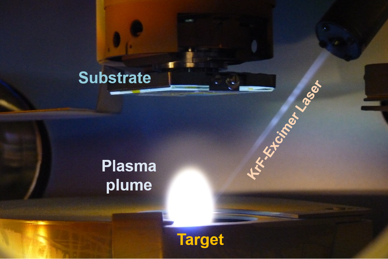
Pulsed Laser Deposition is a physical vapor deposition technique in which compact and dense films (e.g. metal oxides) with a high electronic quality can be grown. In this technique, a pulsed high-power laser is used to evaporate a target of the desired material in a vacuum chamber. The ablation event produces a laser-induced luminous plasma plume that expands rapidly away from the target surface. Consequently, the ablated material is deposited on a substrate.

©HZB/M. Setzpfandt
©HZB/Kölbach
In the Institute for Solar Fuels, we are using this powerful tool to discover and develop new complex multinary metal oxides for the use as photoelectrodes in solar water splitting. Therefore, we have a specially-designed PLD-system (PREVAC, Poland) with the following specifications:
- KrF-Excimer Laser (λ = 248 nm)
- In-situ substrate heating (up to 800°C) in different gas atmospheres (O2, N2, Ar, H2)
- A load-lock with a magazine that holds five positions for targets/substrates for fast transfers to and from the PLD main chamber
- A Target-carousel that holds up to six targets
- A capability to deposit combinatorial material libraries
- An ion beam source for ion assistance of the film growth
- In-situ characterizations: Reflection high energy electron diffraction (RHEED), quartz crystal monitor (QCM), ICCD camera for time-resolved observation of the laser plume, ion energy measurements (time-of-flight method)