New Options for transparent contact electrodes

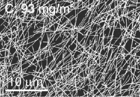
Scanning Electron Microscopy of Nanowires of Silver.
They have diameters around 0,1 micrometer and lenghts
between 5 and 10 micrometern. © ACS Nano 3: 1767-1774
Found in flat screens, solar modules, or in new organic light-emitting diode (LED) displays, transparent electrodes have become ubiquitous. Typically, they consist of metal oxides like In2O3, SnO2, ZnO and TiO2 .
But since raw materials like indium are becoming more and more costly, researchers have begun to look elsewhere for alternatives. A new review article by HZB scientist Dr. Klaus Ellmer, published in the renowned scientific journal Nature Photonics, is hoping to shed light on the different advantages and disadvantages of established and new materials for use in these kinds of contact electrodes.
Metallic (Ag or Cu) or carbon based nanostructures exhibit many interesting properties that could potentially be exploited pending further research.Even graphene, a modified form of carbon, could turn out to be a suitable transparent electrode, since it is both transparent and highly conductive. These properties depend, to a large extent, on the material's composition:graphene, which consists of a single layer of carbon atoms arranged into a hexagonal "honeycomb" grid, is two-dimensional, and, within these dimensions, electrons can freely move about.
According to Ellmer, "these new kinds of materials could be combined with more conventional solutions or find their way into entirely new areas of application." For this to become a reality, researchers have yet to come up with solutions to nanostructure problems like short circuits and continue to illuminate the relevant transport mechanisms. It would also be interesting to determine whether these two-dimensional "electron gases" also form in materials other than graphene. Success ultimately depends on whether or not the new materials prove stable in the long run in their practical application and whether or not they can be produced relatively inexpensively.
Ellmer is sole author of an extensive review article published in Nature photonics online on 30. November 2012, doi: 10.1038/nphoton.2012.282
https://www.helmholtz-berlin.de/pubbin/news_seite?nid=13660;sprache=en
- Copy link
-
BESSY II: How intrinsic oxygen shortens the lifespan of solid-state batteries
Although solid-state batteries (SSBs) demonstrate high performance and are intrinsically safe, their capacity currently declines rapidly. A team from the TU Wien, Humboldt-University Berlin and HZB has now analysed a TiS₂|Li₃YCl₆ solid-state half-cell in operando at BESSY II using a special sample environment that allows for non-destructive investigation under real operating conditions. Data obtained by combination of soft and hard X-ray photoelectron spectroscopy (XPS and HAXPES) revealed a new degradation mechanism that had not previously been identified in solid-state batteries. They have gained some surprising insights, particularly regarding the harmful role played by intrinsic oxygen. This study provides valuable information for improving design and handling of such batteries.
-
Electrocatalysts: New model for charge separation at the solid-liquid interface
Hydrogen is at the heart of the transition to carbon neutrality, as both an energy carrier and a reagent for green chemistry. However, large-scale production of hydrogen via electrolysis, as well as the production of many other chemical products, requires significantly cheaper and more efficient catalysts. A precise understanding of the electrochemical processes that take place at the interface between the solid catalyst and the liquid medium is highly useful for developing better electrocatalysts. In the journal Nature Communications, an European team has now presented a powerful model that determines charge separation at the interface, the formation of the electric double layer and local electric potential variations, and the resulting influence on the catalytic activity.
-
AI-driven Catalyst Discovery: 30 million funding for German consortium
Six partners from research and industry, including Helmholtz-Zentrum Berlin (HZB), the Fritz-Haber-Institute of the Max Planck Society (FHI), BASF, Dunia Innovations, Siemens Energy, and the Technical University Berlin are launching a joint project to accelerate the catalyst discovery. The German Federal Ministry for Science, Technology and Space (BMFTR) is providing €30 million in funding for ASCEND (Accelerated Solutions for Catalysis using Emerging Nanotechnology and Digital Innovation). The research initiative targets the defossilisation of energy-intensive industries while safeguarding industrial competitiveness, with a focus on the chemical sector. The five-year project will start on 1st April 2026.
