Department Interface Design
Examples from current research
Unveiling the Potential of Ambient Air Annealing for Highly Efficient Inorganic CsPbI3 Perovskite Solar Cells
Solar cells based on metal halide perovskites (MHP) with APbX3 [A = CH3NH3+ (MA+), HC(NH2)2+ (FA+), Cs+ and X = I-, Cl-, Br-] as the absorber layer have reached the power conversion efficiency (η) 27% milestone for single junctions, on par with (or above) established, conventional photovoltaic (PV) technologies. Although the long-term stability of MHP solar devices remains a drawback for their upscaling and commercialization, overall, inorganic Cs+ based absorber layers have shown to be less prone to exhibit loss of constituent ions compared to their organic counterparts. Collaborating with HySPRINT, we have studied the chemical properties of CsPbI3 absorbers with or without surface passivation treatments of octylammonium iodide (OAI) and submitted to dry- and ambient air-annealing processing as well as interfaces formed with Spiro-OMeTAD (i.e., a hole transport material, HTM) using hard X-ray photoemission spectroscopy (HAXPES) measured at the HiKE endstation located at BESSY II’s KMC-1 beamline (Figure 1). While the HAXPES study reveals no significant change in chemical composition of the various CsPbI3 samples (Figure 2), an ambient-air-annealing-induced band bending enhancement at the CsPbI3/HTM interface is manifested by symmetric broadening of the investigated photoemission lines (Figure 3), likely caused by the passivation of defect states.

Figure 1: HAXPES detail spectra of the Cs 4d (a, d, g), I 4d (b, e, h), and overlapping Pb 5d/Cs 5s (c, f, i) photoemission lines for the variously treated CsPbI3 films (i.e., OAI-free, dry air, and ambient air annealed) with 0 nm (i.e., bare) (a, b, c), 5 nm (d, e, f), and 20 nm (g, h, i) films of spiro-OMeTAD, respectively. The spectra were measured using 6 keV excitation and normalized to background intensity, with vertical offsets added for clarity. Curve fit results are included.

Figure 2: [Cs]:[Pb]:[I] surface composition of variously treated CsPbI3 films (i.e., OAI-free, dry air and ambient air annealed) with 0 nm (i.e., bare), 5 nm and 20 nm films of HTM, determined by HAXPES measurements employing a) 2 keV and b) 6 keV excitations. Horizontal dashed lines are added to show a [Cs]:[Pb]:[I] composition ratio of 1:1:3 ratio, the nominal stoichiometry of the CsPbI3 samples.

Figure 3: Changes in full-width-half-maximum (FHWM) values of the HAXPES Cs 4d5/2, Pb 5d5/2, I 4d5/2 peaks of CsPbI3 absorbers annealed in dry or ambient air with 0 nm (i.e., bare), 5 and 20 nm films of HTM, measured with excitation energies of (a) 2 and (b) 6 keV, compared to the corresponding peak FHWM values of the bare, OAI-free CsPbI3 sample.
For more details see:
Z. Iqbal, R. Félix, A. Musiienko, J. Thiesbrummel, H. Köbler, E. Gutierrez-Partida, T. W. Gries, E. Hüsam, A. Saleh, R. G. Wilks, J. Zhang, M. Stolterhoft, D. Neher, S. Albrecht, M. Bär, A. Abate, Q. Wang, Unveiling the Potential of Ambient Air Annealing for Highly Efficient Inorganic CsPbI3 Perovskite Solar Cells, J. Am. Chem. Soc. 2024, 146, 4642. DOI: 10.1021/jacs.3c11711
The Energy Level Alignment at the Buffer/Cu(In,Ga)Se2 Thin-Film Solar Cell Interface for CdS and GaOx
Thin-film solar cells based on Cu(In,Ga)Se2 (CIGSe) chalcopyrite light absorbers are a stable, low-band gap bottom device technology for tandem solar cells. Cadmium sulfide (CdS) is the most commonly employed buffer layer between the CIGSe absorber and the emitter in high-efficiency cells. However, the use of a heavy metal, Cd, and parasitic absorption in the short-wavelength range are strong motivation for replacing it by a non-toxic, more transparent alternative buffer. Collaborating with PVcomB, we have studied sputter-deposited GaOx (i.e., oxygen-deficient gallium oxide) films as a potential replacement for the standard CdS buffer layers. Using a combination of lab-based photoemission (XPS, UPS) and inverse photoemission (IPES) spectroscopy measured at the EMIL lab as well as hard x-ray photoemission spectroscopy (HAXPES) measured at BL15XU of Spring-8, we determined the electronic band alignment at the buried GaOx/CIGSe interface and compared it to that of CdS/CIGSe, studied in the same way.
For the GaOx/CIGSe we find a nearly perfect configuration for electron transfer and hole-blocking: (0.04 ± 0.07) eV (i.e., a small spike-like) conduction band offset (CBO) and a (-3.21 ± 0.19) eV (i.e., a large cliff-like) valence band offset (VBO), which suggests a nearly ideal charge-selective contact for electron transfer between the layers. The derived GaOx band gap of (4.80 ± 0.25) eV confirms its utility as a highly transparent buffer layer. However, the GaOx (with x derived to be 1.1 ± 0.1) exhibits considerable (presumably) defect-related occupied states above the valence band maximum. It is proposed that these states may increase charge carrier recombination and limit open circuit voltage in respective devices; also explaining why solar cells with standard CdS buffer outperform devices with GaOx buffer, despite less ideal electronic interface properties (CBO: [-0.18 ± 0.07] eV, VBO: [-0.98 ± 0.15] eV) and the smaller CdS band gap of (2.35 ± 0.22) eV.

Figure 1: UPS (He I or He II excitation as indicated) and IPES spectra of the studied samples: bare CIGSe absorber (after 120 min of mild Ar+ ion treatment) and CIGSe with nominal 50-nm-thick CdS and GaOx buffer layer (after 200 min of mild Ar+ ion treatment). The linear extrapolation of the leading edge positions of the UPS (± 0.10 eV for the bare CIGSe and the CdS/CIGSe sample and ± 0.15 eV for the GaOx/CIGSe sample in absolute position) and IPES (± 0.20 eV in absolute position) spectra (and the computed surface band gap obtained from their differences (± 0.22 eV for the bare CIGSe and the CdS/CIGSe sample and ± 0.25 eV for the GaOx/CIGSe sample)) are indicated. The IPES spectra have had a linear background subtracted; the background was obtained by a fit of the 0 – 2 eV region. The spectra before subtraction are plotted in light grey. Vertical offsets are added for clarity. The leading edges of the UPS and IPES spectra are used to approximate the positions of the valence band maxima and conduction band minima, respectively, relative to the Fermi level. After using measured core level binding energies (not shown) to correct for electronic shifts induced by interface formation, the measurements are used to construct the energy level alignment diagrams shown at right.
For more details see:
D. Valenta, H. A. Yetkin, T. Kodalle, J. Bombsch, R. Garcia-Diez, C. Hartmann, S. Ueda, R. Félix, J. Frisch, L. Bodenstein-Dresler, R. G. Wilks, C. A. Kaufmann, M. Bär, The Energy Level Alignment at the Buffer/Cu(In,Ga)Se2 Thin-Film Solar Cell Interface for CdS and GaOx. Adv. Mater. Interfaces 2024, 11, 2301110. DOI: 10.1002/admi.202301110
A Polymer Bilayer Hole Transporting Layer Architecture for High-Efficiency and Stable Organic Solar Cells
All-solution-processed organic photovoltaic (OPV) devices hold promising cost-effective advantages for the high-throughput preparation of large-area PV devices. The development of solution-processed interface materials that are compatible with non-fullerene acceptor materials would greatly benefit the implementation of widespread OPV applications.
Our collaborators in FAU developed a bilayer hole transport layer (HTL) strategy, consisting of doped PTAA nanoparticles (D-PTAAnp) and PEDOT:PSS, for operation with efficient non-fullerene OPV cells. In order to explore the mechanism behind the improved device performance resulting from the incorporation of the D-PTAAnp layer between a PM6:Y6 active layer and PEDOT:PSS heterointerface, ultraviolet photoelectron spectroscopy (UPS) measurements were conducted on PM6:Y6, PM6:Y6/PEDOT:PSS, and PM6:Y6/DPTAAnp/PEDOT:PSS bilayer HTL samples at HZB’s EMIL and compared to device performance simulations. The secondary electron cutoff (SECO) region and the highest occupied molecular orbital (HOMO) regions are presented in Figure 1a. Summarily, work function (F) values of ~4.7 (± 0.1) eV were determined for the three samples (see Figure 1). The HOMO position of the PM6:Y6 was found to be (-0.4 ± 0.1) eV away from the Fermi (EF) level, while the UPS spectra of the two samples with PEDOT:PSS top layers (i.e., with and without a D-PTAAnp layer) show band tails extending all the way to the EF level (see Figures 1b and 1c), a well-known characteristic of PEDOT:PSS.
While the absolute numbers of energy-level positions derived from device simulations and UPS measurements differ, the UPS data corroborates the presence of a significant HOMO offset between the active layer and PEDOT:PSS and thus further validates the results of the drift-diffusion model used to simulate the J-V curves. However, a D-PTAAnp-induced hole barrier reduction, as predicted by the J-V curve simulations, was not observed in the UPS data. This seeming contradiction can be explained by the inherent specifics of the two characterization approaches. Whereas the J-V characteristic will be affected by electronic structure changes throughout the device stack, the UPS measurements can only probe the top surface (i.e., a few nanometers) of the studied layer stack samples. In light of the J-V curve simulation, which revealed a reduced injection barrier upon D-PTAAnp addition, finding a similar HOMO position for the surface of the PM6:Y6/D-PTAAnp/PEDOT:PSS bilayer HTL sample suggests the presence of a significant electronic structure profile throughout this layer stack.

Figure 1: He I UPS measurements of (a) the secondary electron cut-off (SECO) and (b) the highest occupied molecular orbital (HOMO) energy regions for PM6:Y6, PEDOT:PSS – top (i.e., PM6:Y6/PEDOT:PSS) and Bilayer – top (i.e., PM6:Y6/D-PTAAnp/PEDOT:PSS) samples. c, Spectra in depicted in (b) but presented with a logarithmic intensity scale. d, Energy level positions based on the He I UPS measurements. Work function (Φ) and HOMO values were determined by linear extrapolation of the SECO and leading edge of the valence band, respectively. The margins of uncertainty of the Φ and HOMO values are ± 0.05 and ± 0.1 eV, respectively.
For more details see:
J. Xu, T. Heumüller, V. M. Le Corre, A. Barabash, R. Félix, J. Frisch, M. Bär, C. J. Brabec, A Polymer Bilayer Hole Transporting Layer Architecture for High-Efficiency and Stable Organic Solar Cells. Adv. Mater. Interfaces 2024, 8, 2570. DOI: 10.1016/j.joule.2024.06.013
Chemical Interface Structures in CdS/RbInSe2/Cu(In,Ga)Se2 Thin-Film Solar Cell Stacks
Performance-enhancing heavy alkali-based post-deposition treatments (PDT) of Cu(In,Ga)Se2 (CIGSe) thin-film solar cells absorbers often induce the formation of a Rb- In-Se phase on the CIGSe absorber. Collaborating with PVcomB, we study the effect of layers formed in this way as well as of directly co-evaporated RbInSe2 (RISe) layers using hard X-ray photoelectron spectroscopy (HAXPES). A detailed analysis of the chemical interface structures in CdS/RISe/CIGSe layer stacks is performed, an additional In-Se phase is found to form as a result of direct co-evaporation of a RISe layer on the CIGSe absorber. For the RbF PDT CIGSe absorbers, our study only finds small amounts of Rb and no indication for a RISe layer formation. Examining layer stacks prepared via additional chemical bath deposition (CBD) of CdS reveals a clear impact of the presence of Rb (or of Rb-containing species) on the CIGSe surface. In these cases, an increase of the induction/coalescence period is found at the beginning of the CBD buffer layer growth process and the formation of Cd─Se bonds; thereafter, a more compact CdS layer growth is observed.
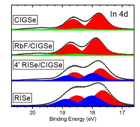
Figure 1: In 4d HAXPES spectra measured using 6keV excitation at BL15XU, SPring-8. The variation in chemical structure resulting from different Rb treatments of the CIGSe surface is clear in the shape of the doublet. The different surface chemical structure leads, ultimately, to variations in the growth of the CdS buffer layer, which influences PV cell performance.
For more details see:
J. Bombsch, T. Kodalle, R. Garcia-Diez, C. Hartmann, R. Félix, S. Ueda, R.G. Wilks, C. A. Kaufmann, M. Bär, Chemical Interface Structures in CdS/RbInSe2/Cu(In,Ga)Se2 Thin-Film Solar Cell Stacks. Adv. Funct. Mater. 2024, 34, 2403685. DOI:10.1002/adfm.202403685