Graphene on titanium carbide triggers a novel phase transition

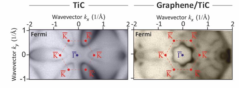
Graphene-induced Lifshitz-transition from a petal-shaped Fermi surface to a gear-shaped hole Fermi surface revealed by comparative full photoemission mapping of the band structures of bare TiC(111) and graphene/TiC(111). © HZB
Researchers have discovered a Lifshitz-transition in TiC, driven by a graphene overlayer, at the photon source BESSY II. Their study sheds light on the exciting potential of 2D materials such as graphene and the effects they can have on neighboring materials through proximity interactions.
Stacking 2D materials has garnered a lot of attention in recent years as it provides a unique opportunity to tailor material properties in a highly controllable manner. However, the influence of 2D materials on the properties of neighboring materials through proximity effects is not yet fully understood. In particular, very sensitive properties such as band gaps in semiconductors and excitonic properties have been observed to be influenced. Fermi surfaces of bulk metals have so far not been among the properties sensitive to a proximity effect.
The Fermi surface of a metal is a mathematical concept to represent the electrons of the highest energy in the material. Only these electrons participate in properties such as electrical conductivity. An important aspect of the Fermi surface is that it represents them in terms of the direction of their movement.
The new study by Andrei Varykhalov and his colleagues at BESSY II shows that a graphene layer can induce a Lifshitz transition in the near-surface region of an underlying metal, TiC: The Fermi surface transforms from a hole-like to an electron-like Fermi surface. The reported change in Fermi surface character is particularly relevant since it changes the orientation of the movement of the electrons and in the presence of a magnetic field it changes the orientation of the macroscopic electric current.
The present finding is an exciting development as it provides a new avenue for controlling and manipulating the electronic properties of materials, which has implications for a range of technological applications, for example designing materials with quantum properties such as high temperature superconductivity.
red.
https://www.helmholtz-berlin.de/pubbin/news_seite?nid=24892;sprache=en
- Copy link
-
Optical innovations for solar modules - which are the most promising?
In 2023, photovoltaic systems generated more than 5% of the world’s electrical energy and the installed capacity doubles every two to three years. Optical technologies can further increase the efficiency of solar modules and open up new applications, such as coloured solar modules for facades. Now, 27 experts provide a comprehensive overview of the state of research and assess the most promising innovations. The report, which is also of interest to stakeholders in funding and science management, was coordinated by HZB scientists Prof. Christiane Becker and Dr. Klaus Jäger.
-
Catalysis research with the X-ray microscope at BESSY II
Contrary to what we learned at school, some catalysts do change during the reaction: for example, certain electrocatalysts can change their structure and composition during the reaction when an electric field is applied. The X-ray microscope TXM at BESSY II in Berlin is a unique tool for studying such changes in detail. The results help to develop innovative catalysts for a wide range of applications. One example was recently published in Nature Materials. It involved the synthesis of ammonia from waste nitrates.
-
BESSY II: Magnetic ‘microflowers’ enhance magnetic fields locally
A flower-shaped structure only a few micrometres in size made of a nickel-iron alloy can concentrate and locally enhance magnetic fields. The size of the effect can be controlled by varying the geometry and number of 'petals'. This magnetic metamaterial developed by Dr Anna Palau's group at the Institut de Ciencia de Materials de Barcelona (ICMAB) in collaboration with her partners of the CHIST-ERA MetaMagIC project, has now been studied at BESSY II in collaboration with Dr Sergio Valencia. Such a device can be used to increase the sensitivity of magnetic sensors, to reduce the energy required for creating local magnetic fields, but also, at the PEEM experimental station, to study samples under much higher magnetic fields than currently possible.
