EMIL
Chemistry laboratory activities
The EMIL Chem Lab will be used by the following groups:
A) Institute for Nanospectroscopy (EM-ISPEK), HZB
B) Department of Crystallography (EM-AKR), HZB
C) Young Investigator Group Interface Design (EE-NI), HZB
D) Fritz-Haber-Institut der Max-Planck-Gesellschaft (FHI), MPI
E) Institute Silicon Photovoltaics (EE-IS), HZB
A) Institute for Nanospectroscopy (EM-ISPEK), HZB
EM-ISPEK will use the EMIL lab as its core-synthesis-lab as well as sample-preparation-lab. Researchers will carry out chemical synthesis of (i) complex noble and transition metallic nanoparticles (such as Au, Ag, Pd, Cu, Ni), (ii) semiconductor quantum dots and nanoparticles (kesterites, heavy & transition metal dichalcogenides), (iii) lanthanide doped nanocrystals as well as (iv) hybrid nanostructured materials (graphene-based materials),(v) Polyol synthesis and microwave-assisted synthesis.
The basic synthetic procedure will involve reduction of metal salts in a sealed flasks. The inert atmosphere and high temperature will be applied where necessary. Other sample preparation will include electroless plating as well as thin film processing for use as transparent conductors.
B) Department of Crystallography (EM-AKR), HZB
Researchers from EM-AKR will use the EMIL Chem lab to carry out synthesis and characterization of compound semiconductor nanocrystals. The whole synthesis will be done inside a dedicated glovebox. The synthesis of nanocrystals will be carried out by hot injection method. This will involve the dissolution of different organometallic salts in a solvent under an inert atmosphere.
This ink will then be deposited on glass substrates by spin coating/doctor blading / printing to produce thin films.
C) Young Investigator Group Interface Design (EE-NI), HZB
Wet chemical treatments: Samples will be frequently submitted to surface treatments in order to: clean their surfaces from adsorbates, remove capping layers, deposit of compound films (kesterites, chalcopyrites), etc. For this purpose, various chemical solutions will be prepared and contained for time periods in the order of minutes. The preparation and use of these solutions would be carried out in the lab. No storage of solutions.
Powder reference preparation: compounds in powder form are pressed to turn them into measurement-suitable pellets.
Material evaporation loading: For e-beam and vapor deposition of thin film layers of various compounds (metal, chalcogenides), the weighing and loading of reagents onto crucibles and evaporator pockets are needed.
D) Fritz-Haber-Institut der Max-Planck-Gesellschaft (FHI), MPI
Researchers from FHI working in the CAT-Lab@EMIL will use the Chem Lab for the following tasks:
- Pellet pressing of powders: Catalytic materials will often be prepared as porous powders and to investigate such catalyst it is required to press them into pellets.
- For electrochemical experiments, such as water electrolysis: Aqueous solutions with known concentration are required. Such solutions will be prepared in the Chem Lab.
- Thin film fabrication: Certain experiments will require the fabrication of thin film materials onto various substrates.
- Calcination of powders: calcination of catalytic powder samples in quartz beakers will be carried out.
E) Institute Silicon Photovoltaics (EE-IS), HZB
From the staff of the Institute EE-IS will use then EMIL-chemistry lab wet chemical methods for preparing various samples (silicon substrates, glass substrates).
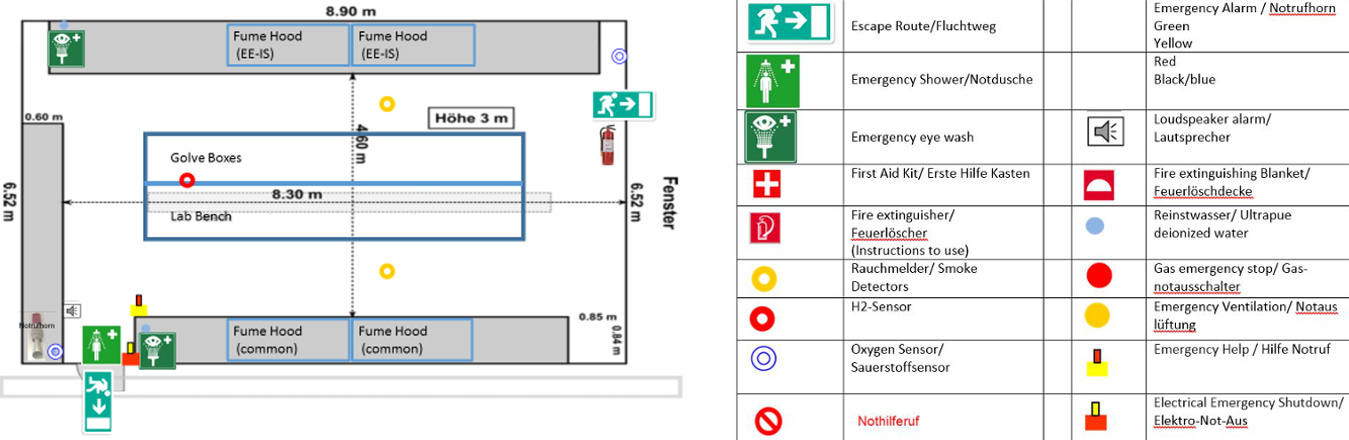
Map of the chemistry lab with emergency features highlighted